Course: QSPI NOR Flash memory VHDL interface
Learn to create a Flash memory controller in VHDL for storing non-volatile data in FPGA projects. This course covers page program (write), read, and erase operations using the quad SPI bus.
Description
This course teaches how to implement a Flash Memory controller in VHDL to interface a 32 MB NOR Flash chip using the Quad Serial Peripheral Interface (QSPI).
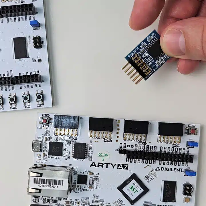
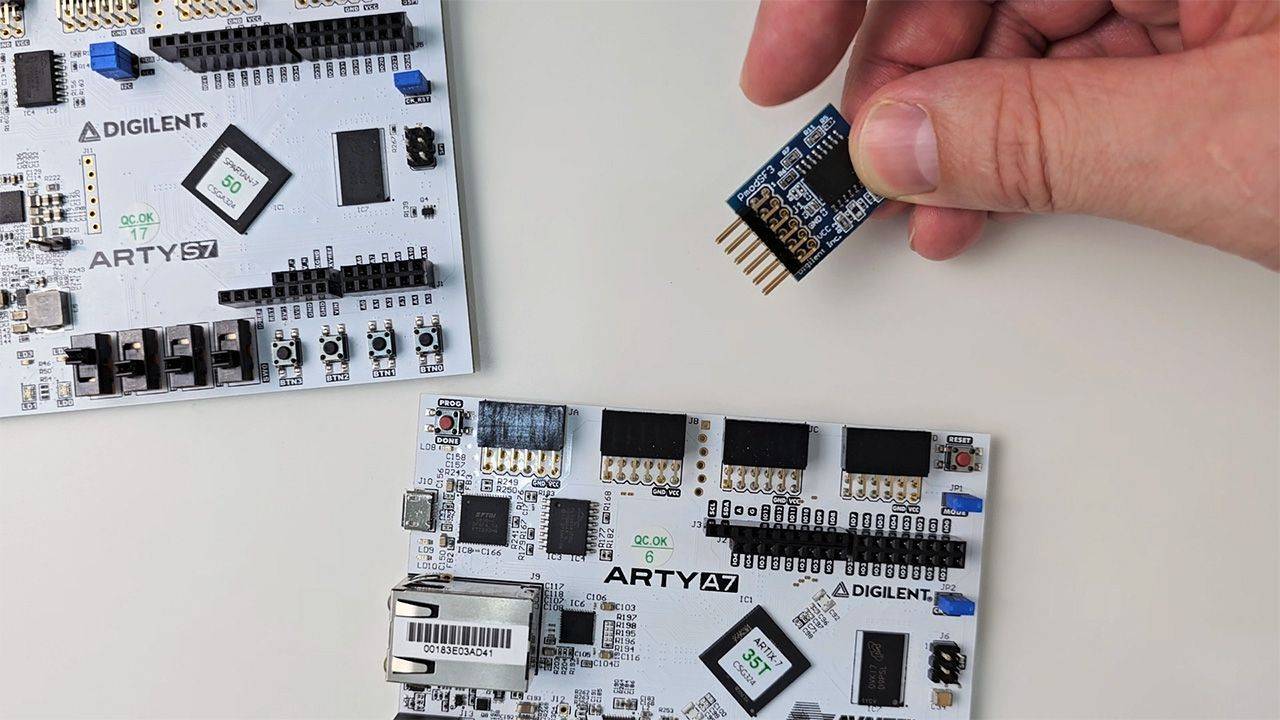
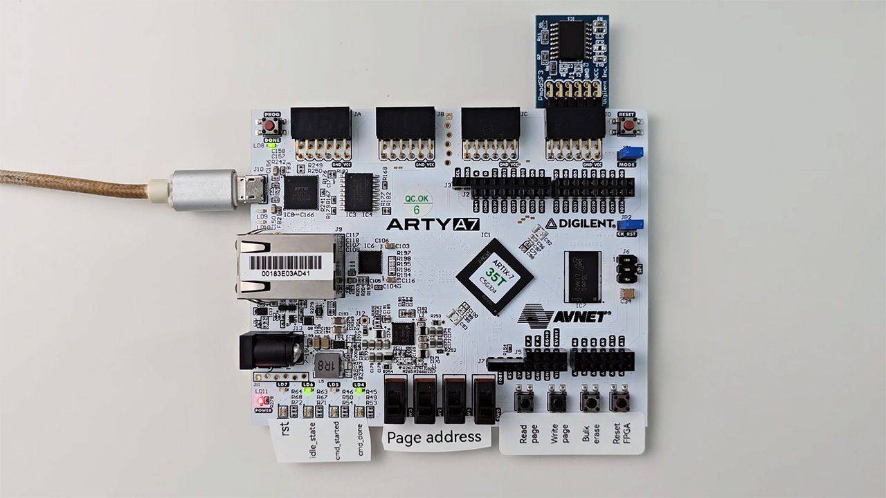
We’ll use the Pmod SF3 module from Digilent, which contains a Micron MT25QL256ABA component, but the methods should work for any QSPI-enabled Flash memory chip. Of course, you would need to read the datasheet for your target chip to obtain the correct command codes.
First, we’ll download the datasheet and Verilog simulation model from Micron. After making some modifications and with the help of a VHDL wrapper, we can utilize it in our VHDL testbench to verify the Flash interface demo project that we’ll create from scratch.
Next, we’ll write a minimal implementation that sends a command using single-bit SPI mode to see that the chip responds. Then, we’ll set the Flash chip in (quad) QSPI mode to increase the transfer speed.
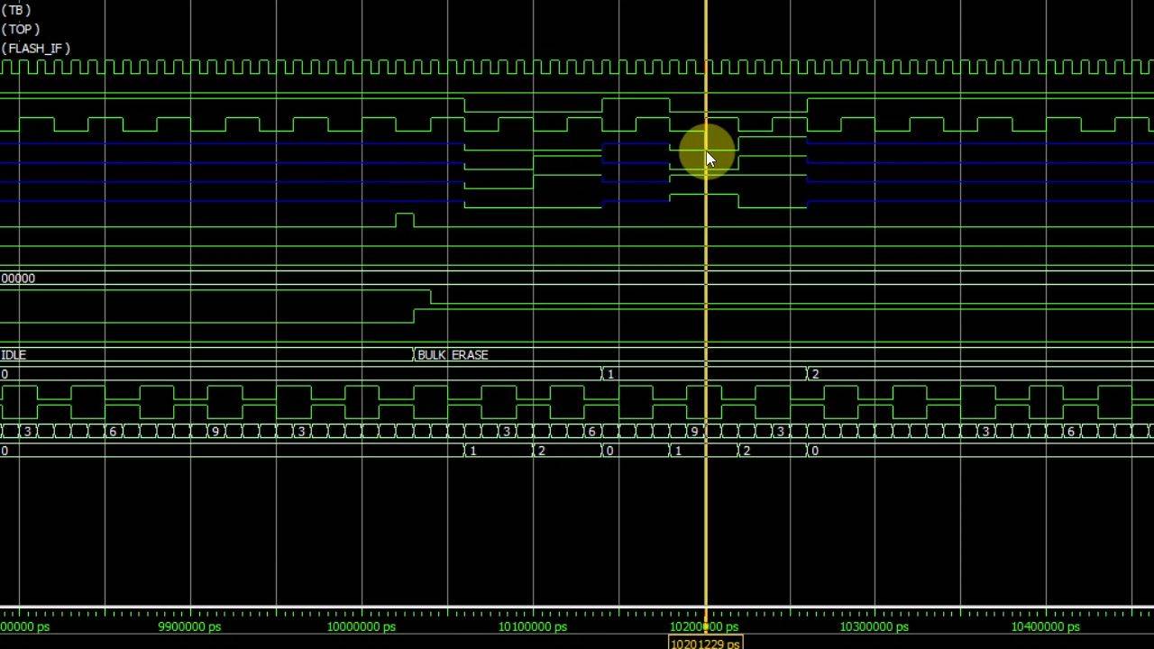
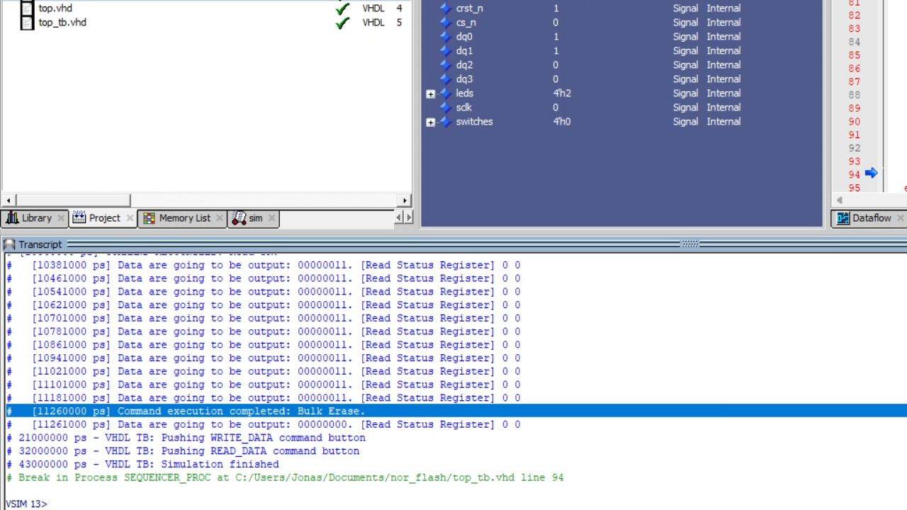
We’ll implement three crucial memory access operations: bulk erase, page program, and page read.
Finally, we shall test that the design works on the FPGA board by feeding data to it from a serial terminal program on the computer. We will see that we can write data to different memory locations and read it back.
See the video below for a preview of selected lessons.
This course is only available in the VHDLwhiz Membership.
The membership subscription gives you access to this and many other courses and VHDL resources.
You pay monthly to access the membership and can cancel the automatic renewal anytime. There is no lock-in period or hidden fees.
Hardware used in the course
- Digilent Pmod SF3: 32 MB Micron MT25QL256ABA8ESF NOR Flash (SKU: 410-340)
Resellers: Digilent, Farnell, Newark, Mouser, DigiKey - Used in the course: Arty A7-35T: Xilinx Artix-7 FPGA
The 35T variant is retired but A7-100T (SKU: 410-319-1) is still sold
Resellers: Digilent, Farnell, Newark, Mouser, DigiKey - Recommended alternative: Arty S7-50: Xilinx Spartan-7 FPGA (SKU: 410-352)
Resellers: Digilent, Farnell, Newark, Mouser, DigiKey
(I’ll provide a constraint file for this board as well, but you can use almost any other FPGA board.)
Software used in the course
I am using Windows 11 in the course. All the other software is available for free for Windows and Linux:
- Questa – Intel FPGA Edition(includes Starter Edition)
(Any version of ModelSim or QuestaSim will work) - AMD Vivado
- Microsoft Visual Studio Code
(Any editor will do) - YAT – Yet Another Terminal
(Any serial (UART) terminal program will do) - The Micron MT25QL256ABA8E0 Serial NOR Flash Verilog simulation model
Course outline
The overview below shows the lessons in this course.

1 - Introduction
Welcome to the course! Let's talk about what you will learn and why NOR and NAND Flash memory chips are so popular among FPGA designers.
2 - The Pmod SF3 and NOR Flash chip
Let's take a closer look at the Digilent Pmod SF3 module with the Micron MT25QL256ABA8ESF NOR Flash memory and its datasheet.
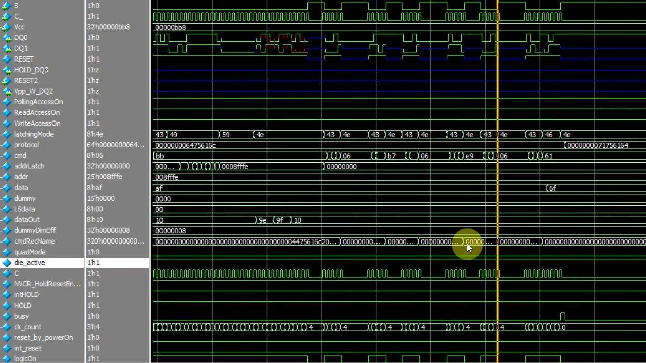
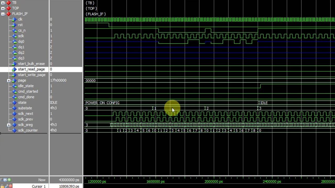
3 - Testing the Micron Verilog simulation model
Micron provides a simulation model of their NOR Flash chip. It would be very beneficial for us if we could get it working in Questa/ModelSim.
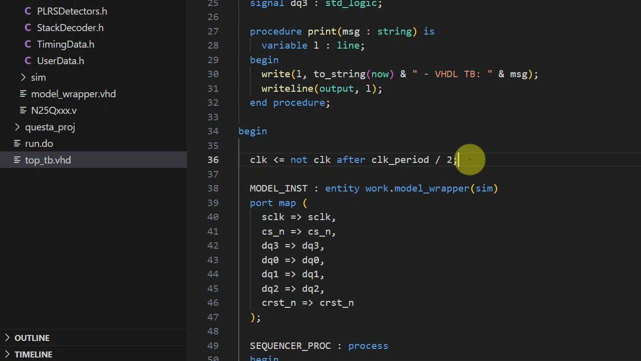
4 - Top-level VHDL testbench with the Verilog model
We'll create a VHDL wrapper for the Verilog simulation module so that we can use it in our testbench as a regular VHDL module.
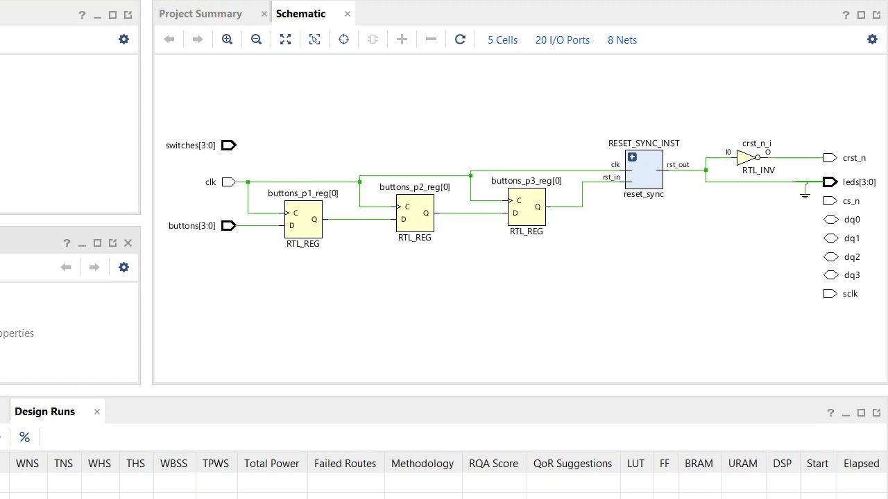
5 - Top module and Vivado project
Let's start defining the top-level VHDL module, add a reset synchronizer to our design, and set up the Vivado project.
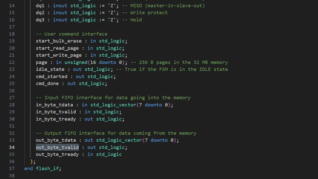
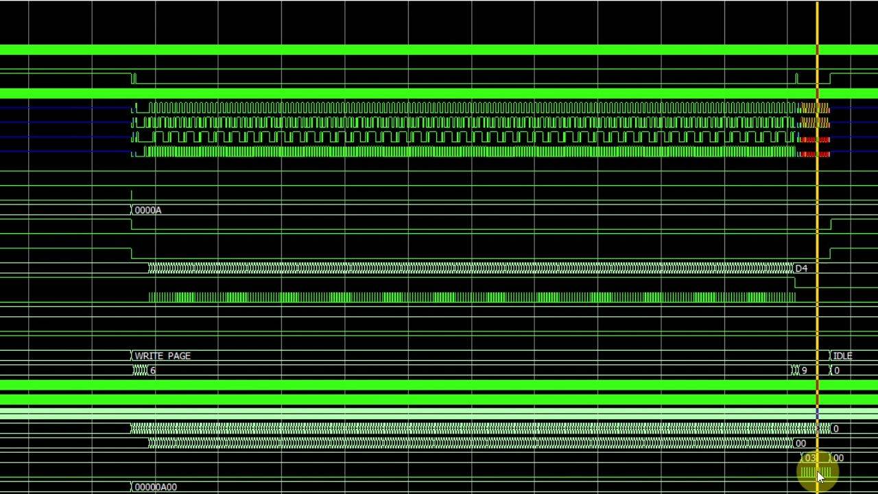
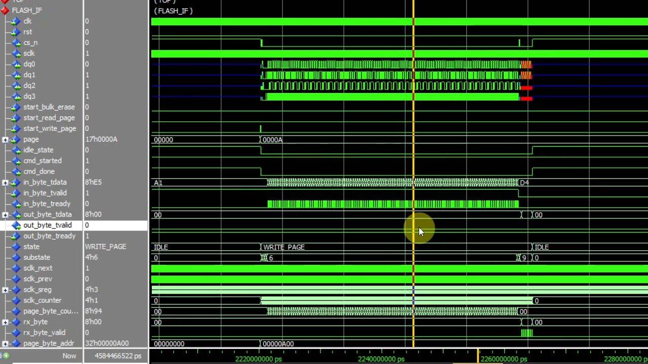
6 - Flash interface module and SCLK generator
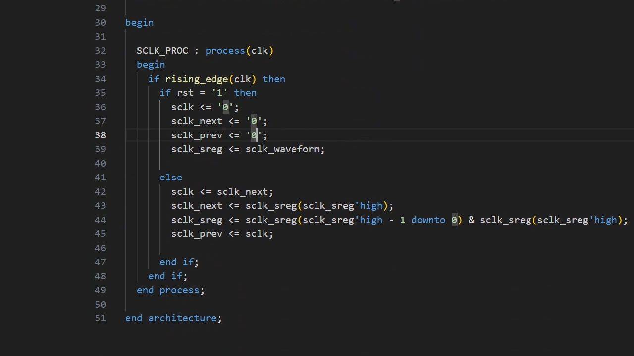
Let's start creating the VHDL module that will communicate with the NOR Flash chip. First, we'll make the process that generates the SPI serial clock.
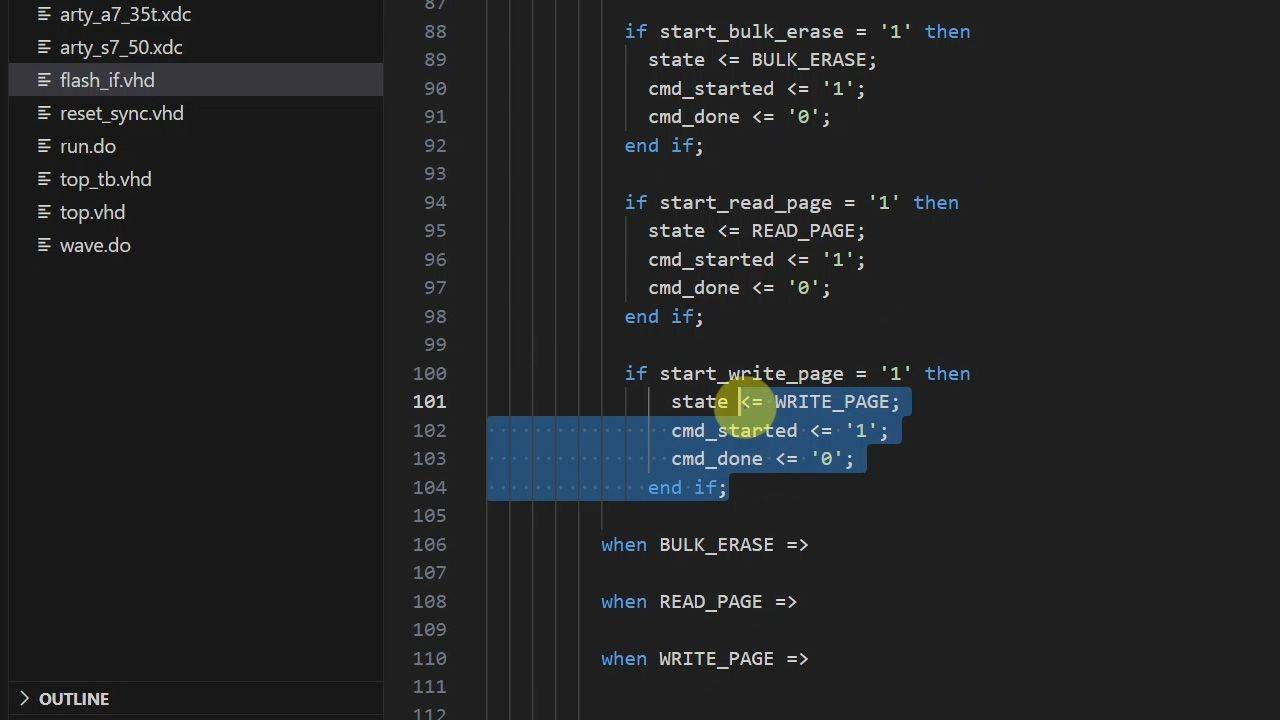
7 - Finite-state machine outline
We'll use pushbuttons to initiate sequences such as bulk erase, write page, or read page. And let's use the output LEDs to indicate the progress of the finite-state machine (FSM).
8 - Send command byte in single-bit mode
After reset, the chip will be in "extended SPI mode." That means we can only send data to it on the dq1 line. We'll make a VHDL procedure to put it in quad SPI mode.
9 - First communication with the chip
Let's try to trigger a response from the Flash chip by sending a command byte that it must respond to. It should reply to the READ ID (9Eh) operation with the manufacturer and device ID numbers.
10 - Transmit using quad SPI mode
We'll create a VHDL procedure to send bytes to the chip using quad SPI mode. First, send the command byte to enable 4-byte addressing. Then, let's start making the bulk erase procedure.
11 - Reading data using quad SPI mode
This VHDL procedure reads bytes from the Flash memory chip. First, we'll use it to read the status register with the write-in-progress (WIP) bit to determine when the erase command completes.
12 - UART host computer interface
We'll include a buffered UART module in the design to allow us to send data from the host computer to be written to the Flash memory and to read data back again.
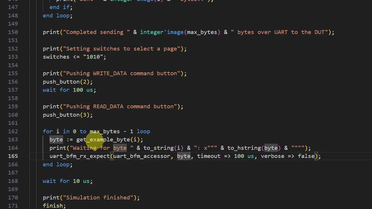
13 - Top-level testbench sending and receiving UART data
To simulate communication with the top module, we'll use a package-based UART bus functional model (BFM) from the VHDLwhiz resource library.
14 - Flash page program VHDL procedure
This VHDL procedure will write (program) a page of 256 bytes with data read from the UART FIFO. In Flash memory, programming only changes bits from 1 to 0, never from 0 to 1.
15 - Reading data from the Flash memory
We'll implement a VHDL procedure that can read a page from the NOR Flash memory using fast quad SPI mode and forward it to the host computer over UART.
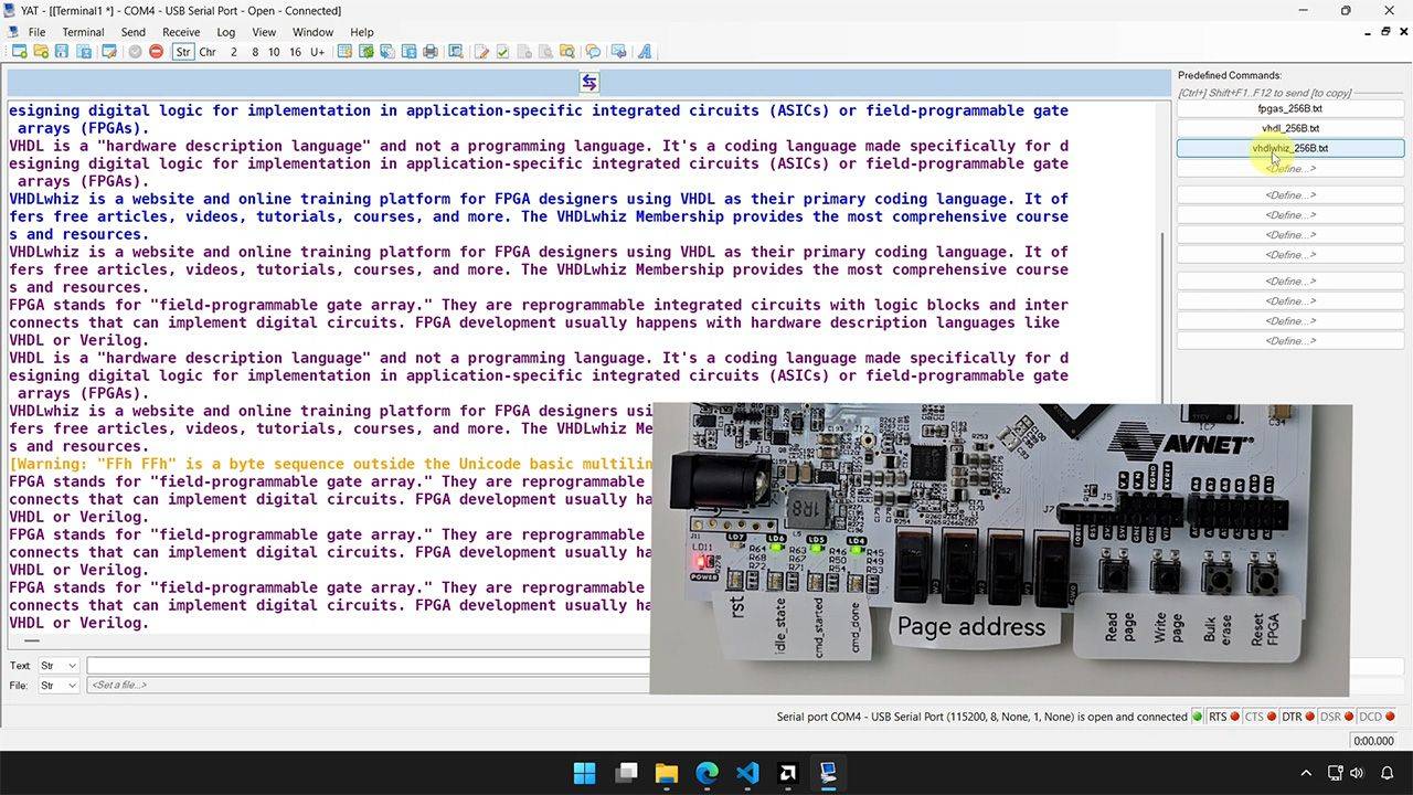
16 - Testing on the FPGA board
Finally, let's implement the completed design in Vivado and test it on the FPGA board. We'll attempt to save text strings in NOR Flash memory pages, then read them back again.
This course is only available in the VHDLwhiz Membership.
The membership subscription gives you access to this and many other courses and VHDL resources.
You pay monthly to access the membership and can cancel the automatic renewal anytime. There is no lock-in period or hidden fees.
Reviews
There are no reviews yet.