Course: I²S audio codec ADC/DAC interface using VHDL and the Xilinx Zynq FPGA
$59
Learn to implement the I²S protocol in VHDL and configure the ADAU1761 ADC/DAC audio codec chip on the Xilinx Zedboard with bare-metal C programming.
Description
This course teaches you how to set up an FPGA system-on-chip (SoC) design for audio processing applications.
First, we create a block design in Vivado and use the Xilinx IIC IP core to interface the configuration port of the Analog Devices ADAU1761 audio codec chip. Then, we export the project to Vitis and write a bare-metal C program to configure its register according to the datasheet.
In the second section of this course, we write a VHDL module that can communicate with the ADAU1761 using the I²S protocol. This module can read audio samples from the ZedBoard’s ADC (analog-to-digital converter) and them back to the DAC (digital-to-analog converter).
With this setup, you can implement any audio processing algorithm in VHDL by manipulating the 24-bit left/right audio samples that are coming from the ADC and going to the DAC.
Finally, in the last section of this course, we create a self-checking testbench for the VHDL design. You will learn to use a bus-functional model (BFM) to simulate the external audio codec chip that the DUT (device under test) talks to, and you will see how to visualize audio data in the simulator waveform.

This course is also available in the VHDLwhiz Membership.
The difference is that when you purchase this product, you get permanent access to the course, while the membership charges a monthly fee to access the content.
Hardware used in the course
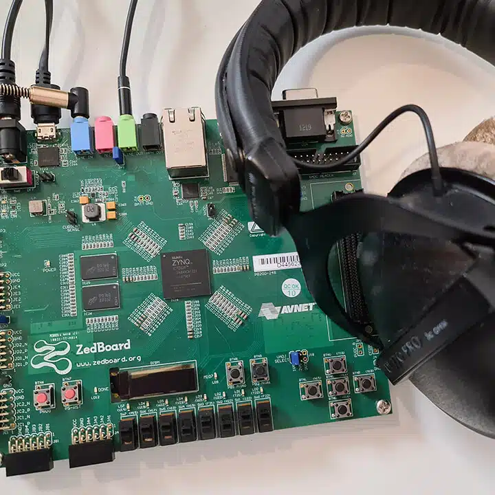
- Xilinx (Avnet) ZedBoard (SKU: AES-Z7EV-7Z020-G)
Resellers: Avnet, Digilent, Mouser, DigiKey
(The ADAU1761 ADC/DAC is on the ZedBoard) - Generic speakers and a mini-jack audio cable
- Generic mini-jack (male) to mini-jack (male) cable
Software used in the course
I am using Windows 10 in the course. All the other software is available for free for Windows and Linux:
- Questa – Intel FPGA Edition(includes Starter Edition)
(Any version of ModelSim or QuestaSim will work) - Xilinx Vivado and Vitis
(Or the implementation software for your FPGA architecture) - Microsoft Visual Studio Code
(Any editor will do)
Course outline
The overview below shows the lessons you can access after purchasing this course.
1 – ZedBoard audio pass-through
We start by creating a system-on-chip (SoC) design in Vivado to communicate with the ADAU1761 audio codec chip’s I²C configuration port. Then we write a C program in Vitis to configure the chip using the Zynq-7000 FPGA’s ARM processor.

1.1 - Project overview
Welcome to this bonus series which is a walkthrough of how I created this month's resource item.

1.2 - Vivado project setup
Let's get started by creating a Vivado project and a folder to store our design files.

1.3 - Vivado block design
Using a block design, we can utilize the free IP cores available in Vivado without coding VHDL.

1.4 - Exporting the hardware to Vitis
To access the custom logic from a C program running on the ARM core, we must first export the hardware configuration from Vivado to Vitis.

1.5 - Creating an application project
Let's first try a template Hello World! application to make sure that the software design flow is working.

1.6 - ADAU1761 I2C configuration
This lesson will go through the C program that writes to the configuration registers on the ADAU1761 chip using I²C.

1.7 - Testing with ILA and speakers
It's time to test the design and see if we can stream audio through the FPGA.
2 – I²S audio interface
In this section, we create an I²S interface module in VHDL. We’ll use it for sending and receiving audio samples through the ADAU1761 audio codec chip on the Xilinx ZedBoard.

2.1 - Project overview
We will create a VHDL module for interfacing an I²S audio codec chip. And we will make a self-checking testbench to verify it in simulation.

2.2 - How I2S works
Before we can create an I²S module, we have to understand how the interface works.

2.3 - Module entity
We'll start on the I²S VHDL module by defining the entity signals and creating the ModelSim project.

2.4 - Synchronize inputs
We need to synchronize the input signals coming from the ADAU1761 chip to the system clock.

2.5 - Audio out and rising/falling edge functions
In this lesson, we create two helper functions and a process for sampling the audio out data.

2.6 - Finite-state machine outline
Let's start by defining the state names and using them in a Case-When statement within a process.

2.7 - Finite-state machine implementation
It's time to complete the state machine and the I²S VHDL module.

2.8 - Vivado block design integration
Let's integrate the finished VHDL module into the Vivado block design, export it to Vitis, and test it on the Xilinx ZedBoard.

2.9 - Testbench challenge
Download the sine_rom module from here:Resources / Example Designs / Sine wave generator using block RAM
3 – I²S BFM and self-checking TB
The final chapter of this course teaches how to create a self-checking testbench (TB). We use a bus-functional model (BFM) to verify the I²S serial audio transceiver, the device under test (DUT).

3.1 - Verification strategy
Before we can start coding, we must agree on the testbench architecture.

3.2 - Testbench package
It's convenient to define shared values and types in a package when the testbench consists of several files.

3.3 - Testbench outline
Let's start creating the testbench file by instantiating the DUT and importing the TB package.

3.4 - Why a manual-check TB isn't good enough
We'll simulate what we have now in ModelSim and look at why we need a self-checking testbench.

3.5 - BFM outline
It's time to start creating the bus functional model (BFM) of the I²S audio codec chip.

3.6 - Generate BCLK and MCLK
Like the physical ADAU1761 chip, the BFM must generate the bit clock and the left/right clock.

3.7 - Generate sine wave samples
To have a sample series that we can easily observe in the waveform, we'll use a sine wave generator.

3.8 - Generate sdata_out
Let's implement the serial audio data output interfacing the device under test.

3.9 - Read sdata_in
We will read the serial audio data from the DUT and show it as an analog signal in the waveform.

3.10 - Close the loop
Finally, we can close the datapath going through the DUT and complete our self-checking testbench.
This course is also available in the VHDLwhiz Membership.
The difference is that when you purchase this product, you get permanent access to the course, while the membership charges a monthly fee to access the content.
Reviews
There are no reviews yet.