Course: Source-synchronous data bus: VHDL design and timing constraints for high-speed FPGA interfaces
Learn to design and implement high-speed source-synchronous parallel data buses in FPGAs using VHDL.
Description
This course teaches how to design and implement high-speed source-synchronous parallel data buses in FPGAs using VHDL. You will gain hands-on experience with timing constraints and experiment with data sampling techniques.
In the course, we create an FPGA sender that produces an output bus consisting of seven parallel data wires and an associated clock signal on the last of the eight pins. Because the bus speed is close to the system clock of the receiver FPGA, asynchronous sampling techniques won’t work. To solve that problem, we use the incoming DQS clock to sample the DQ data signals, and we need to skew the data signals relative to the clock edge using IDELAY elements in the IO buffers in the FPGA.
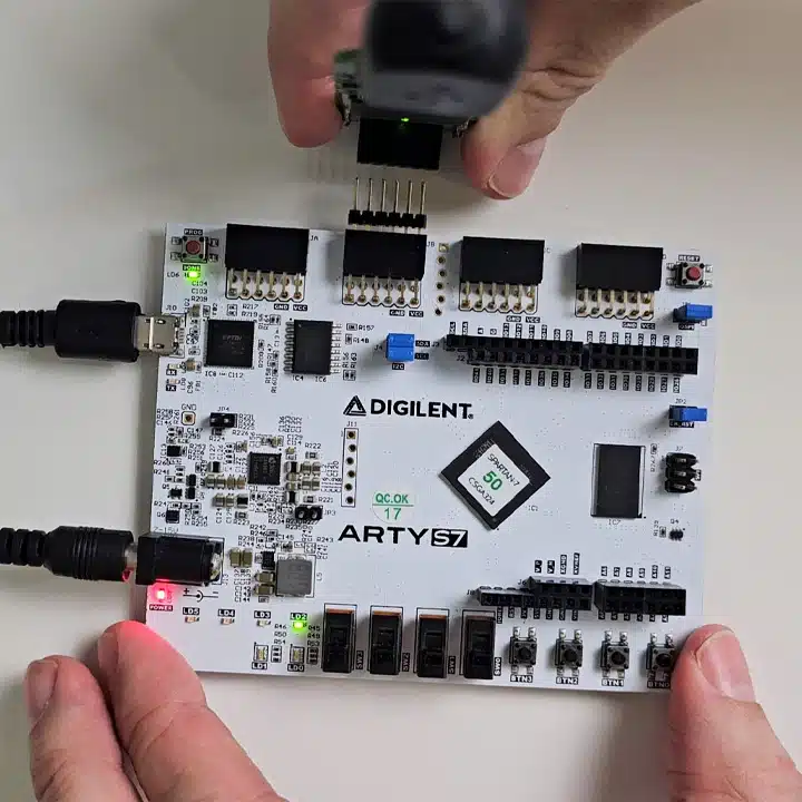
We use two FPGA boards in this course, one as the sender and the other as the receiver. However, you can use a single board for the experiments by implementing the sender and receiver modules in the same FPGA and routing the output pins to some input pins using jumper wires.
This course is only available in the VHDLwhiz Membership.
The membership subscription gives you access to this and many other courses and VHDL resources.
You pay monthly to access the membership and can cancel the automatic renewal anytime. There is no lock-in period or hidden fees.
Hardware used in the course
- Arty S7-50: Xilinx Spartan-7 FPGA (SKU: 410-352)
Resellers: Digilent, Farnell, Newark, Mouser, DigiKey
(You can use other Xilinx/AMD boards) - Lattice iCEstick (SKU: ICE40HX1K-STICK-EVN)
Resellers: Lattice, Farnell, Newark, Mouser, DigiKey
(You can use almost any other FPGA board or the same board as above that sends data to itself)
Software used in the course
I am using Windows 11 in the course. All the other software is available for free for Windows and Linux:
- Questa – Intel FPGA Edition(includes Starter Edition)
(Any version of ModelSim or QuestaSim will work) - AMD Vivado
- Lattice iCEcube2 Design Software
(Or the implementation software for your FPGA architecture) - Microsoft Visual Studio Code
(Any editor will do)
Course outline
The overview below shows the lessons in this course.

1 - Introduction
Welcome to the course! Get ready to experiment with high-speed data buses.

2 - Generator module
Let's start by creating a VHDL module for the sender FPGA that generates known data patterns for easy verification on the receiver side.

3 - Receiver module
The receiver module will sample and check the incoming DQ data signals on the rising edge of the DQS clock. We'll first attempt to treat it as an asynchronous input bus.

4 - iCEstick generator implementation
We'll implement the generator module on the Lattice iCEstick FPGA board. It will act as the sender on the test interface.

5 - Program the iCEstick and check using a logic analyzer
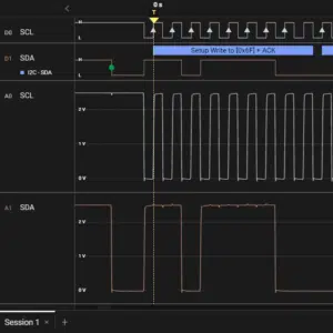
Let's connect a logic analyzer to the iCEstick board to see if we can sample and check the data before completing the receiver FPGA.

6 - Arty S7 asynchronous receiver implementation
We'll implement the receiver module on the Arty S7 FPGA development board. It will act as the receiver for the test interface.

7 - Asynchronous receiver test
Now, we'll connect the two FPGAs and see if the asynchronous receiver approach works well.

8 - Source-synchronous receiver module
Let's convert the receiver module to a source-synchronous design by sending DQS to the clock input on the sampling flip-flops.

9 - Source-synchronous Vivado implementation
We need to make some changes to the top module's pin assignments and constraints to make it work with the source-synchronous receiver module.

10 - Testing without IDELAYs
The first test of the new receiver FPGA implementation will reveal if we have timing issues due to setup and hold time violations.

11 - Using IDELAY2s to skew the data signals
We'll use IDELAY2 elements in the Spartan-7 FPGAs IOBs to skew DQ relative to DQS to sample the data when it's stable.

12 - Testing with variable IDELAYs
Let's test the new implementation using IDELAY2 elements on the data input pins of the interface.

13 - Increasing the speed of the interface
Now that we have the source-synchronous bus design working let's fine-tune the timing constraints and increase the clock speed of the interface.
This course is only available in the VHDLwhiz Membership.
The membership subscription gives you access to this and many other courses and VHDL resources.
You pay monthly to access the membership and can cancel the automatic renewal anytime. There is no lock-in period or hidden fees.


Reviews
There are no reviews yet.