We can construct any other digital logic gate using only NAND gates as building blocks. This is why NAND is known as a universal gate. NAND logic is widely used as the foundation for designing digital circuits in modern integrated chips.
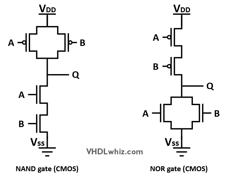
Actually, NOR is also a universal gate, but NAND logic is more prevalent than NOR logic due to its speed and area advantages in CMOS implementation. Even though NOR and NAND both require two nMOS and two pMOS transistors, NAND is preferred because the nMOS transistors are in series, whereas in NOR, the pMOS transistors are in series. nMOS transistors are faster (more conductive) than pMOS and can therefore be made smaller.
Here follows the interactive logic gate implementations of:
- NAND
- NOT (NAND logic)
- AND (NAND logic)
- OR (NAND logic)
- NOR (NAND logic)
- XOR (NAND logic)
- XNOR (NAND logic)
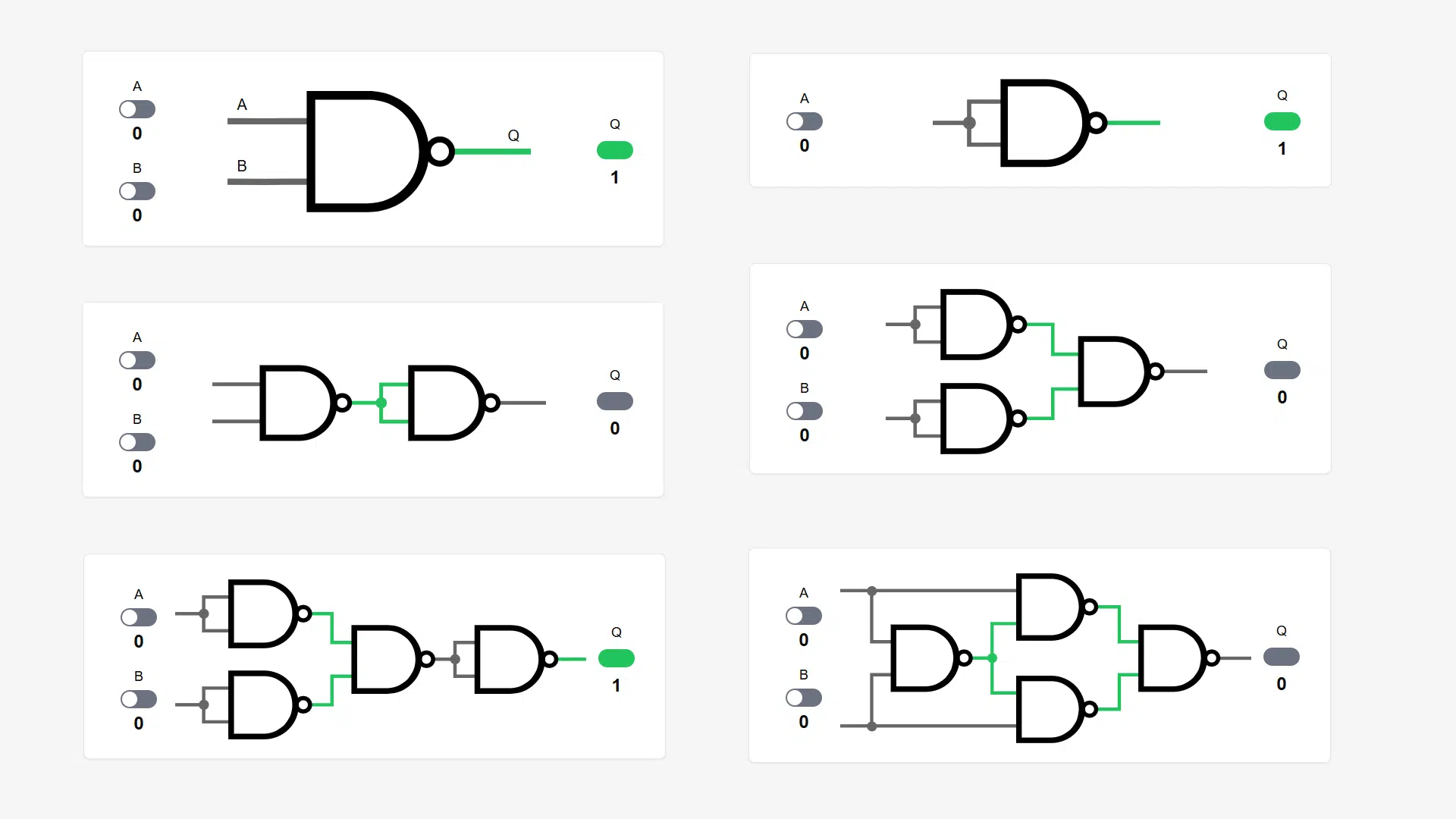
NAND
For reference, this is the NAND gate by itself. Its output is 0 only when both inputs are 1. For all other combinations, the output is 1.
NOT (NAND logic)
You can make an inverter from a NAND gate by tying its inputs together. That works because when A and B are 0, the NAND’s output is 1, and when A and B are 1, the output is 0, precisely the behavior of the inverter.
AND (NAND logic)
An AND gate is just a NAND with an inverted output, and we already know how to make an inverter from NAND, so let’s chain them together to implement AND using NAND logic.
OR (NAND logic)
According to De Morgan’s law, an OR gate is functionally equivalent to a NAND gate with inverters attached to its inputs: \overline{ A \cdot B} = \overline{A} + \overline{B} \implies A + B = \overline{\overline{A} \cdot \overline{B}}
Below is the schematic representation of the formula. We use two NAND inverters on the inputs of another NAND gate to realize the Boolean expression.
NOR (NAND logic)
A NOR gate is, by definition, an OR gate with an inverted output. Therefore, we can make one by placing a NAND inverter after the OR gate we constructed in the previous section. The schematic below shows the resulting four-gate NOR implementation.
XOR (NAND logic)
We can think of XOR as a function that checks if the inputs are different (see the truth table below). Now, let’s explain how this circuit achieves that.
The leftmost NAND will output 0 only if both inputs are 1. It outputs 1 in any other case. The middle two NAND gates compare the output of the leftmost NAND with the A and B inputs.
Let’s focus on the output from the middle NANDs. When A ≠ B, one path becomes active. When A = B, both paths are 1. Under no circumstances are both paths 0.
The rightmost NAND gate takes these two paths as inputs. Since its output is 0 only when both inputs are 1, it effectively detects the case where A = B and outputs 0. When the inputs differ, its output is 1, and our NAND logic implementation of the XOR gate is complete.
XNOR (NAND logic)
We could have created an XNOR gate by placing a NAND inverter after the XOR circuit above. That would also use only five NAND gates, but there’s a better solution that keeps the combinational path at three levels (same as the XOR).
In the circuit below, the two leftmost NANDs, along with the bottom-middle NAND, implement an OR function (see that the OR gate implementation previously in this article is identical). Let’s use Boolean algebra to prove that the circuit implements XNOR.
Given what we already know, the outputs from the mid-level NANDs are \overline{A \cdot B} and A + B.
Combine this with the final NAND, and we get: \overline{\overline{A \cdot B} \cdot (A + B)}
We can apply De Morgan’s law to transform the expression into: \overline{\overline{A \cdot B}} + \overline{A+B}
Simplify the left term and apply De Morgan’s to the right: A \cdot B + \overline{A} \cdot \overline{B} = A \odot B