Did you know that you can construct any other digital logic gate using only NOR gates? You can also do it with NAND logic. That’s why we say that these two are universal gates.
This article shows one way to implement every logic gate using NOR logic, and the schematics are interactive, like a logic gate simulator. You can play with the inputs in the browser to better understand how they work.
Click here for an interactive demo of the seven standard gates
Here follows the logic gate implementations of:
- NOR
- NOT (NOR logic)
- AND (NOR logic)
- NAND (NOR logic)
- OR (NOR logic)
- XOR (NOR logic)
- XNOR (NOR logic)
NOR
Let’s start with the NOR gate itself. Its output is 1 only when both inputs are 0. NOR simply behaves like an OR gate with an inverter on the output.
NOT (NOR logic)
You can make an inverter (NOT gate) by tying the NOR inputs together. Convince yourself by checking the NOR truth table above. When both inputs are 0, the output is 1, and when both are 1, the output is 0. That’s precisely the behavior of an inverter.
AND (NOR logic)
According to De Morgan’s law, an AND gate is functionally equivalent to a NOR gate with inverters attached to its inputs: \overline{ A \cdot B} = \overline{A} + \overline{B} \implies A \cdot B = \overline{\overline{A} + \overline{B}}
Since we already know how to make an inverter from NOR, we can implement the AND gate using three NOR gates, where two act as input inverters.
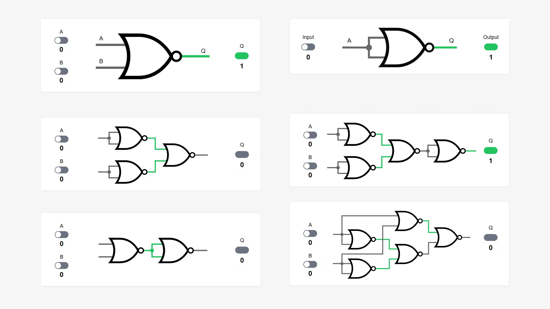
NAND (NOR logic)
A NAND is just an AND with its output inverted. Thus, we can chain together the AND gate from above with the NOR-inverter we created earlier to implement a fully functional NAND gate.
OR (NOR logic)
A NOR is by definition the negation of OR. So, to recover the original OR behavior, we can attach a NOR-inverter to its output.
XOR (NOR logic)
Let’s see how to implement XOR using NOR logic. Instead of deriving the Boolean expression, we’ll use this logical reasoning:
An AND gate detects when both inputs are 1, while a NOR gate detects when both inputs are 0. By passing the outputs of these two gates into a final NOR gate, the output becomes 1 only when A and B have differing values. That’s the XOR behavior.
See if you can spot the AND (NOR implementation) and the two additional NOR gates in the schematic below.
XNOR (NOR logic)
An XNOR gate is just an inverted XOR. So we could have attached a NOR-inverter to the XOR implementation above, and it would have worked. But that’s unnecessarily complicated.
Actually, it makes more sense to create an XOR by inverting the output of the XNOR below, but that circuit will have a longer combinational path than the one above. Both proposed XOR and XNOR implementations have three logic levels, but we only need four NOR gates to implement XNOR. That’s one less than for the XOR.
In the XNOR circuit below, the leftmost NOR gate outputs 1 when both A and B inputs are 0. Let’s call this the all-zero condition.
In the next stage, two additional NOR gates both take all-zero as one input, with A connected to one gate and B to the other. Whenever the all-zero condition is true, it forces both of these NOR gates to output 0, regardless of the value of A or B. Thus, the NOR gates on the second level can only output 1 when the all-zero condition is false and their respective second input is 0.
The NOR gate in the final stage takes the outputs from the previous level as inputs. Because at least one of those inputs will be 1 if A != B, the output from the final NOR will be 1 only if A = B (XNOR behavior).


When I was a Junior in High School in 1968 I purchased some relatively inexpensive 8 pin (round) NOR logic gates and flip flops that used RTL — the basic NOR gate was a Fairchild ul914, and I think the flip flops were ul923. I think they were featured in a magazine, possbily Radio Electronics. Much later I learned that the Apollo program used Farichild RTL gates as well, but in flat pack packaging.