The vast majority of VHDL designs uses clocked logic, also known as synchronous logic or sequential logic. A clocked process is triggered only by a master clock signal, not when any of the other input signals change.
The basic building block of clocked logic is a component called the flip-flop. There are different variants of it, and in this tutorial we are going to focus on the positive-edge-triggered flip-flop with negative reset:
The flip-flop is a sample-and-hold circuit, meaning that it copies the value from the input to the output when the rising edge of the clock signal arrives. The output is then held stable at the sampled value until the next rising edge of the clock, or until the reset signal is pulsed.
This blog post is part of the Basic VHDL Tutorials series.
All clocked processes are triggered simultaneously and will read their inputs at once. At the same time, they will output the results from the last iteration. The clock signal effectively creates timesteps in the data flow. This makes it manageable for the designer to create complex, deep logic. He or she can break down the actions of the algorithm into events that happen on the clock cycles.
Flip-flops or arrays of flip-flops are sometimes referred to as registers; it’s the same thing.
The sensitivity list for clocked processes usually contains only the clock signal. This is because a clocked process is triggered only by a flank on the clock signal. The other input signals won’t cause it to wake up at all.
This is a template for creating a clocked process with synchronous reset:
process(Clk) is
 begin
     if rising_edge(Clk) then
         if nRst = '0' then
             <reset all output signals here>
         else
             <main logic here>
         end if;
     end if;
 end process;
Exercise
In this video tutorial we will learn how to create a clocked process in VHDL:
The final code for the flip-flop testbench:
library ieee;
use ieee.std_logic_1164.all;
use ieee.numeric_std.all;

entity T17_ClockedProcessTb is
end entity;

architecture sim of T17_ClockedProcessTb is

    constant ClockFrequency : integer := 100e6; -- 100 MHz
    constant ClockPeriod    : time    := 1000 ms / ClockFrequency;

    signal Clk    : std_logic := '1';
    signal nRst   : std_logic := '0';
    signal Input  : std_logic := '0';
    signal Output : std_logic;

begin

    -- The Device Under Test (DUT)
    i_FlipFlop : entity work.T17_FlipFlop(rtl)
    port map(
        Clk    => Clk,
        nRst   => nRst,
        Input  => Input,
        Output => Output);

    -- Process for generating the clock
    Clk <= not Clk after ClockPeriod / 2;

    -- Testbench sequence
    process is
    begin
        -- Take the DUT out of reset
        nRst <= '1';

        wait for 20 ns;
        Input <= '1';
        wait for 22 ns;
        Input <= '0';
        wait for 6 ns;
        Input <= '1';
        wait for 20 ns;

        -- Reset the DUT
        nRst <= '0';

        wait;
    end process;

end architecture;
The final code for the flip-flop module:
library ieee;
use ieee.std_logic_1164.all;
use ieee.numeric_std.all;

entity T17_FlipFlop is
port(
    Clk    : in std_logic;
    nRst   : in std_logic; -- Negative reset
    Input  : in std_logic;
    Output : out std_logic);
end entity;

architecture rtl of T17_FlipFlop is
begin

    -- Flip-flop with synchronized reset
    process(Clk) is
    begin

        if rising_edge(Clk) then
            if nRst = '0' then
                Output <= '0';
            else
                Output <= Input;
            end if;
        end if;

    end process;

end architecture;
The waveform window in ModelSim after we pressed run, and zoomed in on the timeline: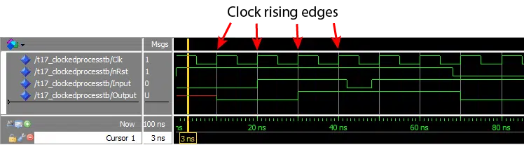
Need the Questa/ModelSim project files?
Let me send you a Zip with everything you need to get started in 30 seconds
Tested on Windows and Linux Loading Gif.. 
Analysis
We can see from the waveform that the output signal is only updated on each rising edge of the clock signal. The input signal is sampled only when the clock signal changes from ‘0’ to ‘1’. The negative dip of the input signal starting at about 45 ns is completely lost. It’s not copied to the output because it’s in between two rising edges of the clock, and therefore it is ignored.
This animation illustrates how the output reacts to the changing input and clock signals:
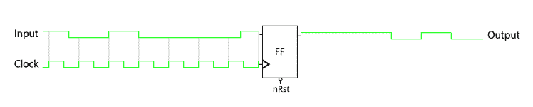
The vertical lines indicate how the input signal is relative to the rising edges of the clock.
Pay special attention to the one positive pulse on the input signal starting at 20 ns. It’s synchronous to the clock and exactly one clock period long. The output doesn’t react instantaneously. It’s delayed by one clock period.
When I was learning VHDL, I found this particularly hard to understand. The rising edge of the clock is synchronous with the input’s rising edge, so how can the flip-flop choose one value or the other?
The simulator uses timesteps to model events in a predictable way, and signals propagate in zero time. Because the flip-flop reads the input in the exact same timestep as it updates the output, it sees the old value of the input and copies it to the output.
Read more about VHDL timesteps here: Delta cycles explained
I should add to this answer that this isn’t really how it works. In the physical world, a signal needs time to propagate, we don’t know exactly when it arrives at the flip-flop. These propagation delays are estimated automatically for us by the software process (place and route), which converts the VHDL code into a netlist.
In reality, the input must be held stable for a few nanoseconds before and after the rising clock edge:

These critical time periods are known as setup and hold time. Fortunately, this is not something you normally have to take into consideration. When working purely with clocked logic, these problems are handled by the software, which turns the VHDL code into a netlist.
Get free access to the Basic VHDL Course
Download the course material and get started.
You will receive a Zip with exercises for the 23 video lessons as VHDL files where you fill in the blanks, code answers, and a link to the course.
By submitting, you consent to receive marketing emails from VHDLwhiz (unsubscribe anytime).
Takeaway
- Clocked processes with synchronized reset only have the clock signal on the sensitivity list
- The
if rising_edge(Clk)ensures that the process only wakes up on rising edges of the clock - In a synchronous design, stuff only happens at the active clock edge
Take the Basic VHDL Quiz – part 3 »
or
Go to the next tutorial »

Hi Jonas!
I’ve seen all your VHDL-Videos on Youtube and currently doing your quiz to check if I actually understood everything. They really made me more confident. Especially the delta-cycles questions gave me a chance to think through everything myself and having a feedback, if it was correct.
Having just finished your quiz (part3) I noticed that you did not cover the topic “setup and hold time” in your Video “How to create a Clocked Process in VHDL”. This seems to be an important topic to me as failing to understand this might quickly lead to hard to find bugs in the actual application. As far as I know these timings are important to write the design constraint files (i.e. *.sdc files in Altera Quartus II for example). Could you do a Video on that topic?
Regards,
Stefan
PS: Thank you for all the tutorials. They were much more helpful then others I’ve seen. Having experienced all the intentinally “buggy programs” fail and how they were fixed, was much easier to learn the rules than just being told “you can’t do this!” (=forgotten minutes later). You focus on the issue, explain why stuff failes, fast-forward on routine work (as loading files into the simulator) while giving an audible summary when doing so. Keep it up!!! 🙂
Hi Stefan,
Thank you for the kind words.
Setup and hold time is indeed important to fully understand. Without knowing about that, you would be clueless when faced with some of the most common place and route errors. When dealing with external interfaces, we must specify the setup and hold time constraints, because the synthesis tool has no way of knowing the limitations of the external signal.
But when dealing only with clocked logic internally in an FPGA, we generally don’t think about setup and hold time when designing. It is handled by the synthesis tool which derives the setup and hold time constraints from the clock frequency and duty cycle. But it is important to understand for the previously mentioned reasons.
I didn’t want to talk too much about these issues when introducing flip-flops to new developers. My fear was that by throwing everything at you at the first mention of FFs, I would overcomplicate things. Therefore, I chose focus on the purely digital, event-driven properties of the FF. Like they behave in the perfect world of the simulator.
By doing so, I may have made the article more confusing to the more curious reader, like yourself. Note that I tried to wash my hands by including a “this isn’t really how it works” paragraph at the end of the blog post (haha).
Anyway, thank you for your comment. Setup and hold times will be talked about in the future in this blog.
Jonas
Hi Jonas, I was reading this post and started to feel confused after reading the ANALYSIS section, where you explain the relationship between data input and clock.
So first I understood that the output is copied from input after one clock cycle (20ns – 30ns interval) because of the timestep of the simulator.
Second, what happens in real life? Let’s assume we don’t have combinational logic. Given the situation at 20ns in the simulation…the data input would be changing in a forbidden zone. If data input is one clock long, data output may be lost?
Hi Dante,
That’s a good question! What happens in the FPGA if we place two flip-flops after each other without any combinational logic between them? How does the timing add up?
Let’s open up the Datasheet for the Xilinx Zynq FPGA family. On page 54 the setup and hold times for the FFs are listed. Hold times after the clock edge range from 0.05 ns to 0.26 ns. Those time intervals are considerably lower than the combined propagation delay and routing delay from one FF to the next. By the time the new value arrives at the second FF, the hold time is already over and the setup time is yet to begin.
The equation is a bit more complicated than that because you have to take into consideration for example that the clock doesn’t arrive at the two FFs exactly at the same time. But you only have to think about these things when communicating with signals that are external to the FPGA. The vendor-specific FPGA tools have exact timing models for the inner workings of the chip, place-and-route will report a failure if there are any timing violations.
When I created this tutorial I didn’t want to talk about setup and hold time, because it’s an advanced subject, and it’s not something you have to think about when designing VHDL for intra-FPGA use. At the same time, I felt I couldn’t mention FFs without mentioning setup and hold time as I did in the Analysis section. It’s an important subject, but fortunately, you don’t have to think about it most of the time.
Hi Jonas,
both article and video are very interesting. However, I’ve a doubt.
With the clock in the sensitivity list, “we” enter into the process only when an event happens to the clock.
Then, If there is a rising edge something happens, otherwise the output is not changed.
What if don’t we put the clock inside the sensitivity list? I mean, the behaviour will be almost the same:
we will continuously enter inside the process but we will modify the output if and only if a rising edge happens.
Best
Hi Umberto,
Intuitively, what you are saying makes sense. But it doesn’t work because that’s a compilation error in VHDL. A process must have a sensitivity list, or it must contain at least one wait-statement.
On the other hand, you could remove the sensitivity list and use a wait-statement instead. The two processes below are equivalent.
process begin if rising_edge(clk) then -- Do something end if; wait on clk; end process; process(clk) begin if rising_edge(clk) then -- Do something end if; end process;Hello Jonas,
This video is unclear.
Could you please add a new clear one here.
BR,
Jaisal
Hi Jaisal,
Sorry about that. Facebook suddenly decided to reduce the quality of this video. I’ve replaced it temporarily with the HD version from YouTube. Please reload the page.
Thanks for reporting.
Jonas
Earlier in the tutorials for sensitivity lists, you mentioned that all signals read by a process must be within the sensitivity list. However, here “Input” is not in the sensitivity list with “Clk”. Would you mind clearing this up for me?
Hello Aaron, that’s a great observation!
In a clocked process with synchronous reset, only the clock signal needs to be in the sensitivity list. It’s an exception from the rule I mentioned earlier.
Let’s see if we can figure out why!
So, in the clocked process, all the other code is wrapped in an
if rising_edge(clk) then. The program only enters it when there is a transition from ‘0’ to ‘1’ on the clock signal. It’s an instantaneous event that completes in a single delta cycle (simulator timestep).Thus, a change in any of the other signals wouldn’t matter. The only thing that will trigger this process is a rising edge on the clock. The clocked process describes an edge-triggered device.
* Code removed *
Can I use the same clock code in my above vhdl code so that Max frequency can be determined? or
I removed the code from your comment because it was lengthy, and I think it is not relevant to the question or the answer.
If I understand you correctly, you want to determine what the max frequency that your VHDL module supports. You won’t find that from the VHDL code or in the simulator.
You can only know the max frequency for a given FPGA architecture after you have implemented the design. That would be in the place-and-route logs or the final timing report.
I have found an example:
What does mean?
clk_d is delay clk by 1 clock cycle ) next) or previous clock state?
Hello, Anna. That depends on where the code resides. If it’s within a clocked process like in the code below,
clk_dis a delayed version ofclkby one clock cycle andclk_ddis delayed by two cycles with respect toclk.process(clk) begin if rising_edge(clk) then clk_d <= clk; clk_dd <= clk_d; end if; end process;On the other hand, if the two lines of code reside directly in the architecture, and not within the context of a process,
clk_dandclk_ddare simply copies ofclkand not delayed at all.Check out this article if you want to learn more about how signal scheduling works in VHDL: Delta cycles explained.
You should join the Facebook group where you can ask questions and discuss problems with thousands of other members! 🙂
dear sir, may you show the vhdl coding for up-down counter with asynchronous reset but synchronous load enable signals.Im really appreatiate it sir.
“The simulator uses timesteps to model events in a predictable way, and signals propagate in zero time. Because the flip-flop reads the input in the exact same timestep as it updates the output, it sees the old value of the input and copies it to the output.”
Could I ask two further questions regarding this statement?
1. I still don’t get why the flip flop sees the old value not the new value. I’m sorry for my disturbance. It’s true I know( from many testbenches and simulations) But could you give a more detailed explanation?
2. Is seeing the old value a common thing? Image a clocked process(rising_edge type), if this process is using a signal that changes with the rising edge of the clock to calculate output, so the process will use the signal’s old value( that is before the rising edge ) or signal’s new value ( that is after the rising edge)