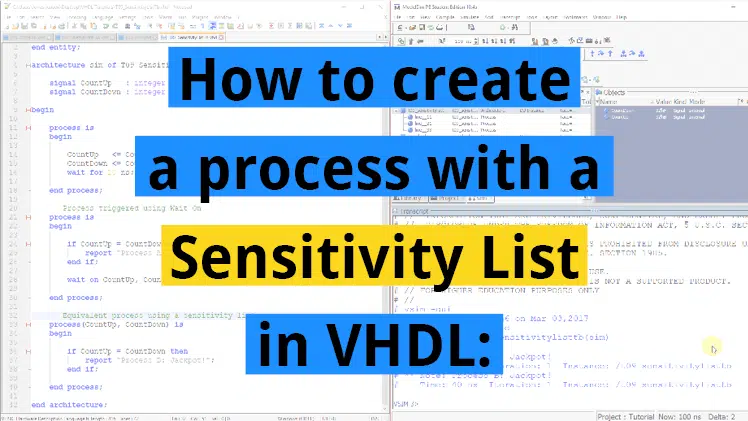
Circular buffers are popular constructs for creating queues in sequential programming languages, but they can also be implemented in hardware. In this article, we will create a ring buffer in VHDL to implement a FIFO in block RAM.
There are many design decisions you will have to make when implementing a FIFO. What kind of interface do you need? Are you limited by resources? Should it be resilient to over-read and overwrite? Is latency acceptable? Those are some of the questions that arise in my mind when asked to create a FIFO.
There exist many free FIFO implementations online, as well as FIFO generators like Xilinx LogiCORE. But still, many engineers prefer to implement their own FIFOs. Because even though they all perform the same basic queue and dequeue tasks, they can be vastly different when taking the details into account.
How a ring buffer works
A ring buffer is a FIFO implementation that uses contiguous memory for storing the buffered data with a minimum of data shuffling. New elements stay at the same memory location from the time of writing until it is read and removed from the FIFO.
Two counters are used to keep track of the location and the number of elements in the FIFO. These counters refer to an offset from the start of the memory space where the data is stored. In VHDL, this will be an index to an array cell. For the rest of this article, we will refer to these counters are pointers.
These two pointers are the head and tail pointers. The head always points to the memory slot that will contain the next written data, while the tail refers to the next element that will be read from the FIFO. There are other variants, but this is the one we are going to use.
Empty state

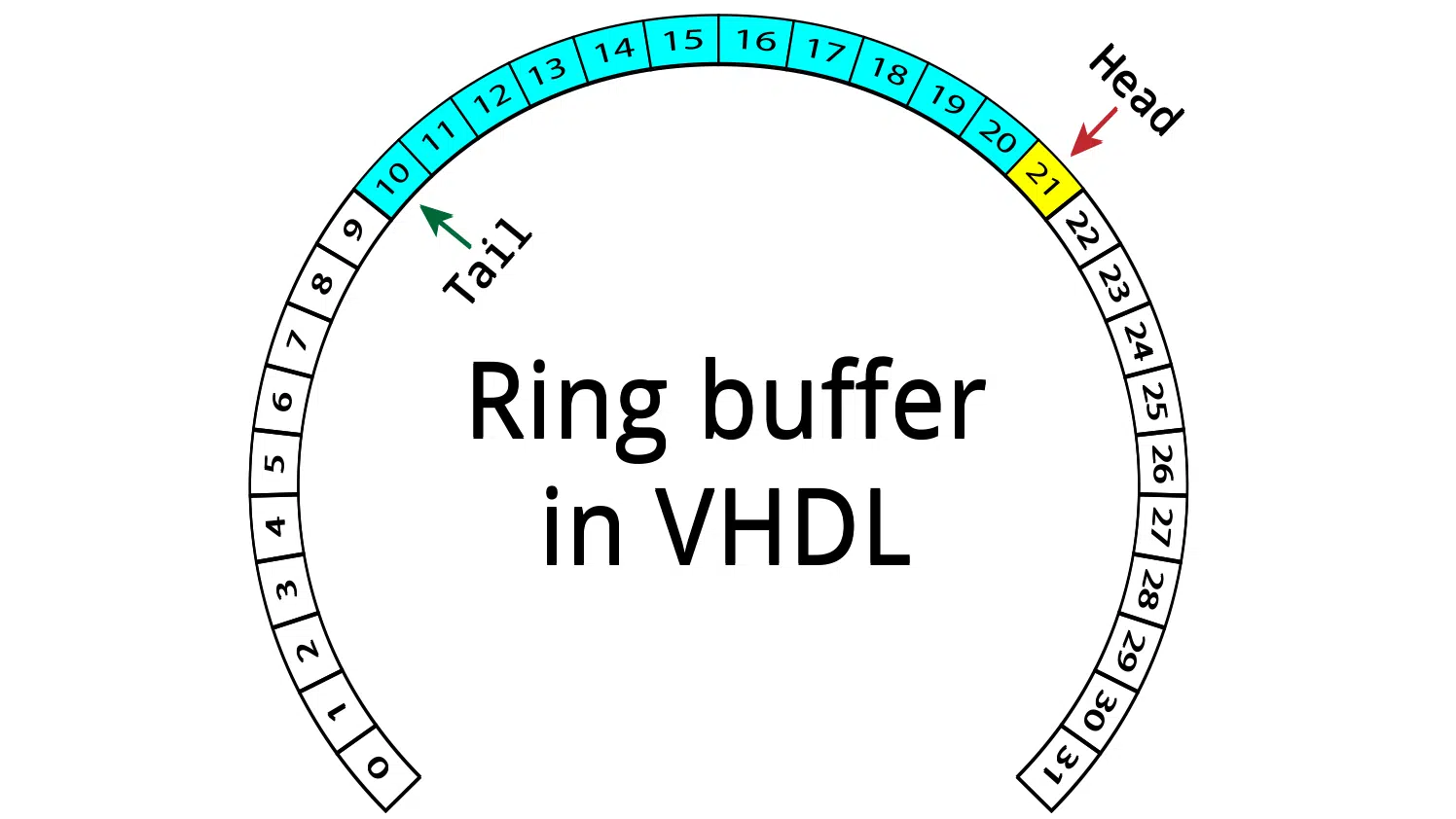
If the head and tail point to the same element, it means that the FIFO is empty. The image above shows an example FIFO with eight slots. Both the head and the tail pointer are pointing to element 0, indicating that the FIFO is empty. This is the initial state of the ring buffer.
Note that the FIFO would still be empty if both pointers were at another index, for example, 3. For each write, the head pointer moves one place forward. The tail pointer is incremented every time the user of the FIFO reads an element.
When either of the pointers is at the highest index, the next write or read will cause the pointer to move back to the lowest index. This is the beauty of the ring buffer, the data doesn’t move, only the pointers do.
Head leads tail

The image above shows the same ring buffer after five writes. The tail pointer is still at slot number 0, but the head pointer has moved to slot number 5. The slots containing data are colored light blue in the illustration. The tail pointer will be at the oldest element, while the head points to the next free slot.
When the head has a higher index than the tail, we can calculate the number of elements in the ring buffer by subtracting the tail from the head. In the image above, that yields a count of five elements.
Tail leads head

Subtracting the head from the tail only works if the head leads the tail. In the image above, the head is at index 2 while the tail is at index 5. Thus, if we perform this simple calculation, we get 2 – 5 = -3, which makes no sense.
The solution is to offset the head with the total number of slots in the FIFO, 8 in this case. The calculation now yields (2 + 8) – 5 = 5, which is the correct answer.
The tail will be forever chasing after the head, that’s how a ring buffer works. Half of the time the tail will have a higher index than the head. The data is stored between the two, as indicated by the light blue color in the image above.
Full state

A full ring buffer will have the tail pointing to the index directly after the head. A consequence of this scheme is that we can never use all of the slots to store data, there has to be at least one free slot. The image above shows a situation where the ring buffer is full. The open, but unusable slot, is colored yellow.
A dedicated empty/full signal could also be used for indicating that the ring buffer is full. This would allow all of the memory slots to store data, but it requires additional logic in form of registers and lookup tables (LUTs). Therefore, we are going to use the keep one open scheme for our implementation of the ring buffer FIFO, as this only wastes cheaper block RAM.
The ring buffer FIFO implementation
How you define the interface signals to and from your FIFO is going to limit the number of possible implementations of your ring buffer. In our example, we are going to use a variation of the classic read/write enable and empty/full/valid interface.
There will be a write data bus on the input side that carries the data to be pushed to the FIFO. There will also be a write enable signal, which when asserted, will cause the FIFO to sample the input data.
The output side will have a read data and a read valid signal controlled by the FIFO. It will also have a read enable signal controlled by the downstream user of the FIFO.
The empty and full control signals are part of the classic FIFO interface, we will use them too. They are controlled by the FIFO, and their purpose is to communicate the state of the FIFO to the reader and writer.
Back pressure
The problem with waiting until the FIFO is either empty or full before taking action is that the interfacing logic won’t have time to react. Sequential logic works on a clock cycle to clock cycle basis, the rising edges of the clock effectively separate the events in your design into timesteps.

One solution is to include almost empty and almost full signals that precede the original signals by one clock cycle. This gives the external logic time to react, even when reading or writing continuously.
In our implementation, the preceding signals will be named empty_next and full_next, simply because I prefer to postfix rather than prefix names.

The entity
The image below shows the entity of our ring buffer FIFO. In addition to the input and output signals in the port, it has two generic constants. The RAM_WIDTH generic defines the number of bits in the input and output words, the number of bits each memory slot will contain.
The RAM_DEPTH generic defines the number of slots that will be reserved for the ring buffer. Because one slot is reserved for indicating that the ring buffer is full, the capacity of the FIFO will be RAM_DEPTH – 1. The RAM_DEPTH constant should be matched to the RAM depth on the target FPGA. Unused RAM within a block RAM primitive will be wasted, it cannot be shared with other logic in the FPGA.
entity ring_buffer is
  generic (
    RAM_WIDTH : natural;
    RAM_DEPTH : natural
  );
  port (
    clk : in std_logic;
    rst : in std_logic;

    -- Write port
    wr_en : in std_logic;
    wr_data : in std_logic_vector(RAM_WIDTH - 1 downto 0);

    -- Read port
    rd_en : in std_logic;
    rd_valid : out std_logic;
    rd_data : out std_logic_vector(RAM_WIDTH - 1 downto 0);

    -- Flags
    empty : out std_logic;
    empty_next : out std_logic;
    full : out std_logic;
    full_next : out std_logic;

    -- The number of elements in the FIFO
    fill_count : out integer range RAM_DEPTH - 1 downto 0
  );
end ring_buffer;
In addition to the clock and reset, the port declaration will include classic data/enable read and write ports. These are used by the upstream and downstream modules for pushing new data to the FIFO, and for popping the oldest element from it.
The rd_valid signal is asserted by the FIFO when the rd_data port contains valid data. This event is delayed by one clock cycle after a pulse on the rd_en signal. We will talk more about why it has to be this way at the end of this article.
Then comes the empty/full flags set by the FIFO. The empty_next signal will be asserted when there are 1 or 0 elements left, while empty is only active when there are 0 elements in the FIFO. Similarly, the full_next signal will indicate that there is room for 1 or 0 more elements, while full only asserts when the FIFO cannot accommodate another data element.
Finally, there is a fill_count output. This is an integer that will reflect the number of elements currently stored in the FIFO. I have included this output signal simply because we will be using it internally in the module. Breaking it out through the entity is essentially free, and the user may choose to leave this signal unconnected when instantiating this module.
The declarative region
In the declarative region of the VHDL file, we will declare a custom type, a subtype, a number of signals, and a procedure for internal use in the ring buffer module.
type ram_type is array (0 to RAM_DEPTH - 1) of
  std_logic_vector(wr_data'range);
signal ram : ram_type;

subtype index_type is integer range ram_type'range;
signal head : index_type;
signal tail : index_type;

signal empty_i : std_logic;
signal full_i : std_logic;
signal fill_count_i : integer range RAM_DEPTH - 1 downto 0;

-- Increment and wrap
procedure incr(signal index : inout index_type) is
begin
  if index = index_type'high then
    index <= index_type'low;
  else
    index <= index + 1;
  end if;
end procedure;
First, we declare a new type to model our RAM. The ram_type type is an array of vectors, sized by the generic inputs. The new type is used on the next line to declare the ram signal that will hold the data in the ring buffer.
In the next block of code, we declare index_type, a subtype of integer. Its range will be indirectly governed by the RAM_DEPTH generic. Below the subtype declaration, we are using the index type to declare two new signals, the head and tail pointers.
Then follows a block of signal declarations that are internal copies of entity signals. They have the same base names as the entity signals but are postfixed with _i to indicate that they are for internal use. We are using this approach because it’s considered bad style to use inout mode on entity signals, although this would have the same effect.
Finally, we declare a procedure named incr which takes an index_type signal as a parameter. This subprogram will be used for incrementing the head and tail pointers, and wrap them back to 0 when they are at the highest value. The head and tail are subtypes of integer, which normally doesn’t support wrapping behavior. We will use the procedure to circumvent this problem.
Concurrent statements
At the top of the architecture, we declare our concurrent statements. I prefer to gather these one-liner signal assignments before the normal processes because they are easily overlooked. A concurrent statement is actually a form of process, you can read more about concurrent statements here:
How to create a Concurrent Statement in VHDL
-- Copy internal signals to output
empty <= empty_i;
full <= full_i;
fill_count <= fill_count_i;

-- Set the flags
empty_i <= '1' when fill_count_i = 0 else '0';
empty_next <= '1' when fill_count_i <= 1 else '0';
full_i <= '1' when fill_count_i >= RAM_DEPTH - 1 else '0';
full_next <= '1' when fill_count_i >= RAM_DEPTH - 2 else '0';
In the first block of concurrent assignments, we are copying the internal versions of the entity signals to the output. These lines will ensure that the entity signals follow the internal versions at the exact same time, but with one delta cycle delay in simulation.
The second and last block of concurrent statements is where we assign the output flags, signaling the full/empty state of the ring buffer. We are basing the calculations on the RAM_DEPTH generic and on the fill_count signal. The RAM depth is a constant that won’t be changing. Therefore, the flags will change only as a result of an updated fill count.
Updating the head pointer
The basic function of the head pointer is to increment whenever the write enable signal is asserted from the outside of this module. We are doing this by passing the head signal to the previously mentioned incr procedure.
PROC_HEAD : process(clk)
begin
  if rising_edge(clk) then
    if rst = '1' then
      head <= 0;
    else

      if wr_en = '1' and full_i = '0' then
        incr(head);
      end if;

    end if;
  end if;
end process;
Our code contains an additional and full_i = '0' statement to protect against overwrites. This logic may be omitted if you are certain that the data source will never attempt to write to the FIFO while it’s full. Without this protection, an overwrite will cause the ring buffer to become empty again.
If the head pointer is incremented while the ring buffer is full, the head will be pointing to the same element as the tail. Thus, the module will “forget” the contained data, and the FIFO fill appears to be empty.
By evaluating the full_i signal before incrementing the head pointer, it will only forget the overwritten value. I think this solution is nicer. But either way, if overwrites ever happen, it’s indicative of a malfunction outside of this module.
Updating the tail pointer
The tail pointer is incremented in a similar manner as the head pointer, but the read_en input is used as the trigger. Just like with the overwrites, we are protecting against over-reads by including and empty_i = '0' in the Boolean expression.
PROC_TAIL : process(clk)
begin
  if rising_edge(clk) then
    if rst = '1' then
      tail <= 0;
      rd_valid <= '0';
    else
      rd_valid <= '0';

      if rd_en = '1' and empty_i = '0' then
        incr(tail);
        rd_valid <= '1';
      end if;

    end if;
  end if;
end process;
Additionally, we are pulsing the rd_valid signal on every valid read. The read data is always valid on the clock cycle after rd_en was asserted, if the FIFO wasn’t empty. With this knowledge, there isn’t really any need for this signal, but we will include it for convenience. The rd_valid signal will be optimized away in synthesis if it’s left unconnected when the module is instantiated.
Inferring block RAM
To make the synthesis tool infer block RAM, we have to declare the read and write ports in a synchronous process without reset. We will read and write to the RAM on every clock cycle, and let the control signals handle the usage of this data.
PROC_RAM : process(clk)
begin
  if rising_edge(clk) then
    ram(head) <= wr_data;
    rd_data <= ram(tail);
  end if;
end process;
This process doesn’t know when the next write will happen, but it doesn’t need to know. Instead, we are just writing continuously. When the head signal is incremented as a result of a write, we start writing to the next slot. This will effectively lock in the value that was written.
Updating the fill count
The fill_count signal is used for generating the full and empty signals, which in turn are used for preventing overwrite and over-read of the FIFO. The fill counter is updated by a combinational process that is sensitive to the head and tail pointer, but those signals are only updated at the rising edge of the clock. Therefore, the fill count will also change immediately after the clock edge.
PROC_COUNT : process(head, tail)
begin
  if head < tail then
    fill_count_i <= head - tail + RAM_DEPTH;
  else
    fill_count_i <= head - tail;
  end if;
end process;
The fill count is calculated simply by subtracting the tail from the head. If the tail index is greater than the head, we have to add the value of the RAM_DEPTH constant to get the correct number of elements that are currently in the ring buffer.
The complete VHDL code for the ring buffer FIFO
library ieee;
use ieee.std_logic_1164.all;

entity ring_buffer is
  generic (
    RAM_WIDTH : natural;
    RAM_DEPTH : natural
  );
  port (
    clk : in std_logic;
    rst : in std_logic;

    -- Write port
    wr_en : in std_logic;
    wr_data : in std_logic_vector(RAM_WIDTH - 1 downto 0);

    -- Read port
    rd_en : in std_logic;
    rd_valid : out std_logic;
    rd_data : out std_logic_vector(RAM_WIDTH - 1 downto 0);

    -- Flags
    empty : out std_logic;
    empty_next : out std_logic;
    full : out std_logic;
    full_next : out std_logic;

    -- The number of elements in the FIFO
    fill_count : out integer range RAM_DEPTH - 1 downto 0
  );
end ring_buffer;

architecture rtl of ring_buffer is

  type ram_type is array (0 to RAM_DEPTH - 1) of
    std_logic_vector(wr_data'range);
  signal ram : ram_type;

  subtype index_type is integer range ram_type'range;
  signal head : index_type;
  signal tail : index_type;

  signal empty_i : std_logic;
  signal full_i : std_logic;
  signal fill_count_i : integer range RAM_DEPTH - 1 downto 0;

  -- Increment and wrap
  procedure incr(signal index : inout index_type) is
  begin
    if index = index_type'high then
      index <= index_type'low;
    else
      index <= index + 1;
    end if;
  end procedure;

begin

  -- Copy internal signals to output
  empty <= empty_i;
  full <= full_i;
  fill_count <= fill_count_i;

  -- Set the flags
  empty_i <= '1' when fill_count_i = 0 else '0';
  empty_next <= '1' when fill_count_i <= 1 else '0';
  full_i <= '1' when fill_count_i >= RAM_DEPTH - 1 else '0';
  full_next <= '1' when fill_count_i >= RAM_DEPTH - 2 else '0';

  -- Update the head pointer in write
  PROC_HEAD : process(clk)
  begin
    if rising_edge(clk) then
      if rst = '1' then
        head <= 0;
      else

        if wr_en = '1' and full_i = '0' then
          incr(head);
        end if;

      end if;
    end if;
  end process;

  -- Update the tail pointer on read and pulse valid
  PROC_TAIL : process(clk)
  begin
    if rising_edge(clk) then
      if rst = '1' then
        tail <= 0;
        rd_valid <= '0';
      else
        rd_valid <= '0';

        if rd_en = '1' and empty_i = '0' then
          incr(tail);
          rd_valid <= '1';
        end if;

      end if;
    end if;
  end process;

  -- Write to and read from the RAM
  PROC_RAM : process(clk)
  begin
    if rising_edge(clk) then
      ram(head) <= wr_data;
      rd_data <= ram(tail);
    end if;
  end process;

  -- Update the fill count
  PROC_COUNT : process(head, tail)
  begin
    if head < tail then
      fill_count_i <= head - tail + RAM_DEPTH;
    else
      fill_count_i <= head - tail;
    end if;
  end process;

end architecture;
The code above shows the complete code for the ring buffer FIFO. You can fill out the form below to have the Questa project files, as well as the testbench, emailed to you instantly.
The testbench
The FIFO is instantiated in a simple testbench to demonstrate how it works. You can download the source code for the testbench along with the ModelSim project by using the form below.
Need the Questa/ModelSim project files?
Let me send you a Zip with everything you need to get started in 30 seconds
Tested on Windows and Linux Loading Gif.. 
The generic inputs have been set to following values:
- RAM_WIDTH: 16
- RAM_DEPTH: 256
The testbench first resets the FIFO. When the reset is released, the testbench writes sequential values (1-255) to the FIFO until it’s full. Finally, the FIFO is emptied before the test completes.
We can see the waveform for the complete run of the testbench in the image below. The fill_count signal is displayed as an analog value in the waveform to better illustrate the fill level of the FIFO.
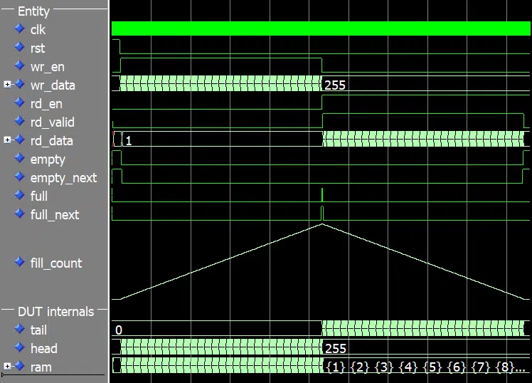
The head, the tail, and the fill count are 0 at the start of the simulation. At the point where the full signal is asserted, the head has the value 255, and so does the fill_count signal. The fill count only goes up to 255 even though we have a RAM depth of 256. That’s because we are using the keep one open method to distinguish between full and empty, as we discussed earlier in this article.
At the turning point where we stop writing to the FIFO and start reading from it, the head value freezes while the tail and fill count start to decrease. Finally, at the end of the simulation when the FIFO is empty, both the head and the tail have the value 255 while the fill count is 0.
This testbench should not be considered adequate for anything other than demonstration purposes. It doesn’t have any self-checking behavior or logic to verify that the output from the FIFO is correct at all.
We will use this module in next week’s article when we dive into the subject of constrained random verification. This is a different testing strategy from the more commonly used directed tests. In short, the testbench will perform random interactions with the DUT (device under test), and the DUT’s behavior has to be verified by a separate testbench process. Finally, when a number of predefined events have occurred, the test is complete.
Click here to read the follow-up blog post:
Constrained random verification
Synthesizing in Vivado
I synthesized the ring buffer in Xilinx Vivado because it’s the most popular FPGA implementation tool. However, it should work on all FPGA architectures that have dual-port block RAM.
We have to assign some values to the generic inputs to be able to implement the ring buffer as a stand-alone module. This is done in Vivado by using the Settings → General → Generics/Parameters menu, as shown in the image below.
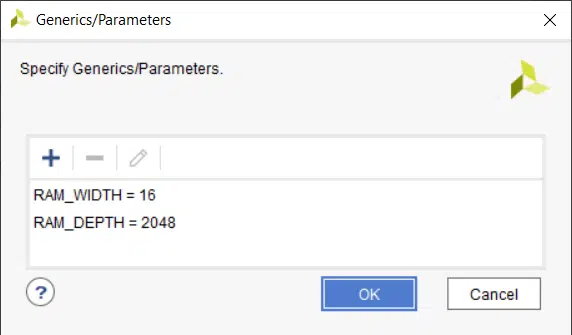
The value for the RAM_WIDTH is set to 16, which is the same as in the simulation. But I have set the RAM_DEPTH to 2048 because this is the max depth of the RAMB36E1 primitive in the Xilinx Zynq architecture that I have chosen. We could have selected a lower value, but it still would have used the same number of block RAMs. A higher value would have resulted in more than one block RAM being used.
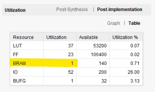
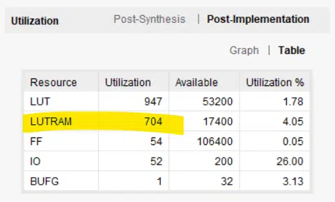
The image below shows the post-implementation resource usage, as reported by Vivado. Our ring buffer has indeed consumed one block RAM and a handful of LUTs and flip-flops.
Ditching the valid signal
You may be asking yourself if the one clock cycle delay between the rd_en and the rd_valid signal actually is necessary. After all, the data is already present on rd_data when we assert the rd_en signal. Can’t we just use this value and let the ring buffer skip to the next element on the next clock cycle as we read from the FIFO?

Strictly speaking, we don’t need the valid signal. I included this signal just for convenience. The crucial part is that we have to wait until the clock cycle after we asserted the rd_en signal, otherwise that RAM won’t have time to react.
Block RAM in FPGAs are fully synchronous components, they need a clock edge both to read and write data. The read and write clock doesn’t have to come from the same clock source, but there has to be clock edges. Furthermore, there can be no logic between the RAM output and the next register (flip-flops). This is because the register that is used to clock the RAM output is inside of the block RAM primitive.

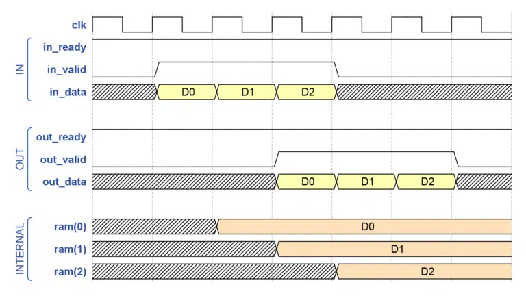
The image above shows at timing diagram of how a value propagates from the wr_data input in our ring buffer, through the RAM, and finally appears on the rd_data output. Because each signal is sampled on the rising clock edge, it takes three clock cycles from we start driving the write port before it appears on the read port. And an additional clock cycle passes before the receiving module can utilize this data.
Reducing the latency
There are ways to mitigate this problem, but it comes at the cost of additional resources used in the FPGA. Let’s try an experiment to cut one clock cycle delay from the read port of our ring buffer. In the code snippet below we have changed the rd_data output from a synchronous process to a combinational process that is sensitive to the ram and tail signal.
PROC_READ : process(ram, tail)
 begin
   rd_data <= ram(tail);
 end process;
Unfortunately, this code cannot be mapped to block RAM because there may be combinational logic between the RAM output and the first downstream register on the rd_data signal.
The image below shows the resource usage as reported by Vivado. The block RAM has been replaced by LUTRAM; a form of distributed RAM implemented in LUTs. LUT usage has skyrocketed from 37 LUTs to 947. Lookup tables and flip-flops are more expensive than block RAM, that’s the whole reason why we have block RAM in the first place.
There are many ways to implement a ring buffer FIFO in block RAM. You may be able to save the extra clock cycle by using another design, but it will cost in form of extra supporting logic. For most applications, the ring buffer presented in this article will be sufficient.
Update:
How to create a ring buffer FIFO in block RAM using the AXI ready/valid handshake
In the next blog post, we will create a better testbench for the ring buffer module by using constrained random verification.
Click here to read the follow-up blog post:
Constrained random verification
Need the Questa/ModelSim project files?
Let me send you a Zip with everything you need to get started in 30 seconds
Tested on Windows and Linux Loading Gif..


Hi VHDLwhiz,
Firstly thank you for your sharing ring buffer fıfo design code. I am a student and try to learn and understand VHDL. The work that I am working on now is about designing data exchanging on UART(RS-232) with this using ring buffer fıfo. I use buffer and rs232 design code as a component and combine them. If necessary RS232 component code, I can send it later. But it doesn’t work and I couldn’t find and understand where the problem is. Could you please help me? Thank you
** Code removed **
Hello Yakup,
Nice to hear from you, and great that you found my blog to be helpful!
I edited your comment to remove the 340 lines of code because it’s not really going the help looking at it. Instead, you should create a testbench and simulate the module before you implement it on the FPGA.
If you have a testbench and it still doesn’t work, there probably is a difference between your simulation and the real environment on the FPGA. In that case, you should debug by first getting the UART TX working, and then the UART RX. When you are confident that the UART is working, you can start looking at the ring buffer FIFO.
You should join my Facebook group where you can ask questions like yours and discuss VHDL with other students:
https://www.facebook.com/groups/vhdlwhiz/
I also have a free 5-day testbench course which starts next week, but you have to register before March 9, 2020, to attend:
https://academy.vhdlwhiz.com/testbench-challenge
Hi, Thank you for this post !
I have a Question…I understand if the deepth is 256 only the fifo will be full with 255 values, so if I need the all 256 values are complete what I must to change in the code ?? I am testing the code for a project and I send 16384 values and every 256 values ( 256, 512,768,..etc) are not written in the FIFO..so I need all values been written. The final values that I recibe next of read the fifo are 16.128 ( 16.384- 256=16.128) and no 16384.
If you need to store 256 values at once in the FIFO, the RAM_DEPTH generic must be set to 257 or more. The only downside is that it may occupy two block RAMs, rather than one (depending on the FPGA’s RAM depth). In that case, you could set it to 512, and it would consume the same number of resources.
Block RAM cannot be shared with other logic. If you use only some of it, the rest is wasted.
An alternative for you is to rewrite the FIFO implementation to use dedicated “full” and “empty” signals, rather than the keep-one-slot-open scheme. Then, you can use the 256 slots, at the cost of additional control logic.
What tool do you use to create such pretty and accurate timing diagrams as the two that I see in this article?
I use wavedrom.com to generate the diagram. Then I download it as SVG before editing it in Adobe Illustrator. I usually increase the text size and add a few arrows and explanations.
Hi Jonas, great article, I will use it for my academic project, it seems much simpler than the Xilinx Fifo Generator, and I don’t like the “black box” effect of Xilinx generator 🙂
However, the main reason to change to your code is that sometime I want to write back the data I read directly inside the FIFO. In fact, on the first passes, I want to get/read all the data inside the FIFO, but I don’t want to delete them. However, I want to delete them on the second/last pass.
I made a simple simulation, it seems to work, can you confirm that I can connect a signal directly from the output of the fifo to the input, and rise the signals rd_en and wr_en in the same time ? Of course, I will use a mux to manage the wr_data input to be able to put new data, or to activate the write back…
Thanks in advance for your help,
Charly
Hello Charly,
It’s great that you found my block RAM FIFO useful in your academic project.
Your assumption is correct that it’s possible to connect the
rd_dataoutput to thewr_datainput. But you have to make sure that the data coming fromrd_datais valid before you assertwr_en. The data appears onrd_datawith one clock cycle delay after you assertrd_en. That’s how block RAM works, and it’s evident from our VHDL code.Perhaps you can connect the
rd_validsignal towr_eninstead. Therd_validsignal is always in sync withrd_data.Another solution is to add an additional read port with an address input. Then you will consume twice as many RAM primitives because the FIFO uses both read/write ports. But if RAM resource usage is not an issue, it can make your implementation simpler.
Add these signals to the entity:
And an additional RAM read process to the architecture:
PORT_B_PROC : process(clk)
begin
  if rising_edge(clk) then
    if rd_en_b = '1' then
      dout_b <= ram(addr_b);
    end if;
  end if;
end process;
You will have to keep track of the read address and how many elements that are in the FIFO, but you don’t have to delete anything to read.
Everything look fine. Just out of curiosity how do you add in the right way the ram, tail and head in the DUT internal in the ModelSim simulator. I add the ram and there is no data in the wave window at all.
Thank you.
Hello Elik,
If you haven’t already, download the example project by entering your email address in the “Need the ModelSim project files?” form above on this page.
Extract the Zip that you receive in your email inbox to somewhere.
Then run the run.do file that’s in the project folder by entering this in the ModelSim console:
(Replace the path with the one to your extracted folder.)
After that, you can type “runtb” in the ModelSim console, and the waveform should appear, including the
ram, thetail, and theheadsignals.These instructions are also shown in the “How to run.txt” and “How to run.gif” file in the downloadable example.
Thank you. I might not explained my self. I meant how manually without the script to add the ram and so it will show the data?
Thank you.
Hi VHDLwhiz,
Thank you very much! This article is very helpful for my work. I have a question? How could I read the data from the buffer and get the maximum value?
Please kindly suggest!
You can create a separate process that continuously stores the max value in a signal. Try merging the code below into the ring_buffer_tb.vhd file to see what I mean.
  signal max_val : std_logic_vector(RAM_WIDTH - 1 downto 0);

begin

  MAX_VAL_PROC : process(clk)
  begin
    if rising_edge(clk) then
      if rst = '1' then
        max_val <= (others => '0');

      else
        if rd_valid = '1' and  unsigned(rd_data) > unsigned(max_val) then
          max_val <= rd_data;
        end if;

      end if;
    end if;
  end process;
I guess you want to reset the
max_valat some point, perhaps after emptying the FIFO. I will leave that as an exercise.You can do this! 😀👍
Thank you very much J. J. Jensen
I follow the way you show me.
This is my result. I could not show my simulation here. Max value appear after fill_count 2 clocks. I add the finish signal to expect could finish the work of code 1 clock after its appear but It not works. Can you check my code and suggest me the better way?
Here is my code. I set the finish signal appear after empty 1 clock.
begin
if rising_edge(clk) then
if reset =’1′ and finish = ‘0’ then
counter <= 0;
max_val <= std_logic_vector(to_unsigned(0,10));
else
if counter = 0 then
counter <= counter +1;
max_val <= std_logic_vector(to_unsigned(0,10));
MAX unsigned(max_val) then
max_val =16 then
counter <=0;
else
counter <= counter +1;
end if;
end if;
end if;
end if;
end process;
HOANG
Hello Jonas Julian Jensen,
This article is so great.
Please suggest me How could I combine all 16-bit rd_data into my 256-bit out data
example: 16 16-bit rd_data –> 256-bit out data
I appreciate your recommend.
Thank you,
NGUYEN
Hello, Nguyen. I guess you have already figured it out since I replied to your comment after a few days. But here’s how you can do it using the ampersand concatenation operator:
type s16_arr_type is array (0 to 15) of std_logic_vector(15 downto 0); signal s16_arr : s16_arr_type; signal s256 : std_logic_vector(255 downto 0); begin -- Concatenate the smaller vectors using the & operator s256 <= s16_arr(15) & s16_arr(14) & s16_arr(13) & s16_arr(12) & s16_arr(11) & s16_arr(10) & s16_arr(9) & s16_arr(8) & s16_arr(7) & s16_arr(6) & s16_arr(5) & s16_arr(4) & s16_arr(3) & s16_arr(2) & s16_arr(1) & s16_arr(0);Thank you very much!
Your article is very useful for my academic project .
Thanks for this article. I am implementing an antique/vintage computer in VHDL from its original IBM Automated Logic Diagrams, implementing the very same logic, at the same clock and cycle speeds as (and optionally faster than) the original – and need to use a PC as a support platform for the lights, switches and I/O devices. That means that multiple original computer sections may be vying for access to the 115,200 bps UART port from the Digilent FPGA development board to transmit state information and data to the PC and thus could *briefly* overrun it. This silo design will help nicely (along with my own design with an arbiter and single character buffers and associated FSMs that can wait for prioritized access to this silo, that will then hook into a UART to send the data. Saved me some time, and probably frustration as well.
https://www.computercollection.net/index.php/ibm-1410-fpga-implementation/
Hello, Jay. That’s an impressive project! Implementing a 1960’s computer sounds like a lot of fun (and a lot of work). And thanks for documenting everything on your blog. I have bookmarked it.
Hello, how do you declare this signals in the code?
RAM_ANCHO: 16
PROFUNDIDAD_RAM: 256
I tried with vector but it said error
Hello. I’m not sure what you mean. Use the INTEGER type, perhaps. But I think it’s more of a general beginner’s question than related to the content of this blog post.
Maybe you should check out the free basic VHDL course:
https://vhdlwhiz.com/basic-vhdl-tutorials/
Or post a question in VHDLwhiz’s free Facebook group:
https://www.facebook.com/groups/vhdlwhiz/
Make sure to include more information and code examples of what you are trying to do. That makes it easier for people to understand your problem and give you a proper answer.
Hi M. Jensen, and thank you for all your helpful ressources and articles.
I am myself implementing a FIFO for a CAN FD and your code helped me well. I managed to use the whole size of the RAM and thus removing the “one open” using the code below (modification in uppercase)
If tail and head are equal, the FIFO is either full or empty. The flag empty_next tells then which case it is, removing the uncertainty. Here, if it is not empty and both are equal then it is the head that got to the tail so the FIFO is full. The full signal can be extended to RAM_SIZE.
This works well in my case. I would be glad to hear if there is any flaw in my code.
As you discovered, you can use additional logic to differentiate between full and empty states. The code looks correct, but the only way to find out for sure is to write a proper testbench.
You would need to test the regular corner cases. The testbench I supplied in the downloadable Zip doesn’t check anything.
Great work so far! 😎👍
Sir, wouldn’t it be enough to just use the full or empty flag? If wr_en =1 and full= 0 , write the value to memory and if it is the last memory block, it should immediately set the full flag to 1, why do we pull it 1 clock later? You do not do such a thing in your example with Axi.
That’s a great question! Why do we need to alert the data source and sink that FIFO will be empty or full before it happens?
It’s because both parties sample the control signals at the exact same time, on the rising clock edge.
Thus, an upstream module that’s writing data into the FIFO won’t be able to sample and react to the ‘full’ signal before it’s too late. When it sees that ‘full’ is asserted, it has already been ‘1’ for one clock period, and the upstream module may have attempted to write to the FIFO while it was full.
AXI’s read/valid handshake, on the other hand, works differently. There, the sender and receiver must examine the ready/valid signals at each rising clock edge to find out if a data transfer happened during the previous clock cycle. It’s a clever signaling that allows the sender and receiver to limit the data transfer or run at full speed.
The full/full_next/empty/empty_next and ready/valid are different flow control schemes. The former uses more signals, but the latter is tricky to implement.
A very simple question I just cant get my head around.
In the process to write and read data, you say that it does not matter that we do this continuously. But even if “wr_en” is 0, then we will still write “some” random data to the RAM or what am I missing?
—————————————–
PROC_RAM : process(clk)
begin
if rising_edge(clk) then
ram(head) <= wr_data;
rd_data <= ram(tail);
end if;
end process;
—————————————
Yes, definitely. That process writes something to the ram(head) slot on every clock cycle. But we only increment the head index if wr_en is ‘1’. If wr_en wasn’t ‘1’ we just overwrite the same slot again until it is.
We have to keep doing that because it would be too slow to stop and check. Then we wouldn’t be able to write one item to the FIFO on every clock cycle while still stopping in time. We just write on every cycle and check on the next if it was valid data.
A consequence of this method is that we always need to keep at least one RAM slot open, so the max words we can store is RAM_DEPTH – 1.
Great question, btw.!
Thank you for the quick reply!
I understand…I could see after I wrote that the location of the head pointer is just overwritten ever clock cycle, but as soon as wr_en is ‘1’, it samples whatever data is on wr_data and stores it and the head pointer is incremented.
That leads me to my question, what you mean that by “…… check on the next if it was valid data.”?
I just reads it as data is stored and we have moved on to the next empty FIFO slot.
Thank you.