I was a little annoyed by the peculiarities of the AXI interface the first time I had to create logic to interface an AXI module. Instead of the regular busy/valid, full/valid, or empty/valid control signals, the AXI interface uses two control signals named “ready” and “valid”. My frustration soon changed to awe.
The AXI interface has built-in flow control without using additional control signals. The rules are easy enough to understand, but there are a few pitfalls one has to account for when implementing the AXI interface on an FPGA. This article shows you how to create an AXI FIFO in VHDL.
AXI solves the delayed-by-one-cycle problem
Preventing over-read and overwrite is a common problem when creating data stream interfaces. The issue is that when two clocked logic modules communicate, each module will only be able to read the outputs from its counterpart with one clock cycle delay.

The image above shows the timing diagram of a sequential module writing to a FIFO which uses the write enable/full signaling scheme. An interfacing module writes data to the FIFO by asserting the wr_en signal. The FIFO will assert the full signal when there isn’t room for another data element, prompting the data source to stop writing.
Unfortunately, the interfacing module has no way of stopping in time as long as it’s using only clocked logic. The FIFO raises the full flag exactly at the rising edge of the clock. Simultaneously, the interfacing module attempts to write the next data element. It can’t sample and react to the full signal before it’s too late.
One solution is to include an extra almost_empty signal, we did this in the How to create a ring buffer FIFO in VHDL tutorial. The additional signal precedes the empty signal, giving the interfacing module time to react.
The ready/valid handshake
The AXI protocol implements flow control using only two control signals in each direction, one called ready and the other valid. The ready signal is controlled by the receiver, a logical '1' value on this signal means that the receiver is ready to accept a new data item. The valid signal, on the other hand, is controlled by the sender. The sender shall set valid to '1' when the data presented on the data bus is valid for sampling.
Here comes the important part: data transfer only happens when both ready and valid are '1' at the same clock cycle. The receiver informs when it’s ready to accept data, and the sender simply puts the data out there when it has something to transmit. Transfer occurs when both agree, when the sender is ready to send and the receiver is ready to receive.

The waveform above shows an example transaction of one data item. Sampling occurs on the rising clock edge, as is usually the case with clocked logic.
Implementation
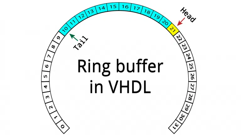
There are many ways to implement an AXI FIFO in VHDL. It could be a shift register, but we will use a ring buffer structure because it’s the most straightforward way to create a FIFO in block RAM. You can create it all in one giant process using variables and signals, or you can split the functionality into multiple processes.
This implementation uses separate processes for most of the signals that have to be updated. Only the processes that need to be synchronous are sensitive to the clock, the others use combinational logic.
Need the Questa/ModelSim project files?
Let me send you a Zip with everything you need to get started in 30 seconds
Tested on Windows and Linux Loading Gif.. 
The entity
The entity declaration includes a generic port which is used for setting the width of the input and output words, as well as the number of slots to reserve space for in the RAM. The capacity of the FIFO is equal to the RAM depth minus one. One slot is always kept empty to distinguish between a full and an empty FIFO.
entity axi_fifo is
  generic (
    ram_width : natural;
    ram_depth : natural
  );
  port (
    clk : in std_logic;
    rst : in std_logic;

    -- AXI input interface
    in_ready : out std_logic;
    in_valid : in std_logic;
    in_data : in std_logic_vector(ram_width - 1 downto 0);

    -- AXI output interface
    out_ready : in std_logic;
    out_valid : out std_logic;
    out_data : out std_logic_vector(ram_width - 1 downto 0)
  );
end axi_fifo;
The first two signals in the port declaration are the clock and reset inputs. This implementation uses synchronous reset and is sensitive to the rising edge of the clock.
There’s an AXI style input interface using the ready/valid control signals and an input data signal of generic width. Finally comes the AXI output interface with similar signals as the input has, only with reversed directions. Signals belonging to the input and output interface are prefixed with in_ or out_.
The output from one AXI FIFO could be connected directly to the input of another, the interfaces fit perfectly together. Although, a better solution than stacking them would be to increase the ram_depth generic if you want a larger FIFO.
Signal declarations
The first two statements in the declarative region of the VHDL file declare the RAM type and its signal. The RAM is dynamically sized from the generic inputs.
-- The FIFO is full when the RAM contains ram_depth - 1 elements
type ram_type is array (0 to ram_depth - 1)
  of std_logic_vector(in_data'range);
signal ram : ram_type;
The second block of code declares a new integer subtype and four signals from it. The index_type is sized to represent exactly the depth of the RAM. The head signal always indicates the RAM slot which will be used in the next write operation. The tail signal points to the slot which will be accessed in the next read operation. The value of the count signal is always equal to the number of elements currently stored in the FIFO, and count_p1 is a copy of the same signal delayed by one clock cycle.
-- Newest element at head, oldest element at tail
subtype index_type is natural range ram_type'range;
signal head : index_type;
signal tail : index_type;
signal count : index_type;
signal count_p1 : index_type;
Then comes two signals named in_ready_i and out_valid_i. These are merely copies of the entity outputs in_ready and out_valid. The _i postfix just means internal, it’s part of my coding style.
-- Internal versions of entity signals with mode "out"
signal in_ready_i : std_logic;
signal out_valid_i : std_logic;
Finally, we declare a signal which will be used to indicate a simultaneous read and write. I will explain its purpose later in this article.
-- True the clock cycle after a simultaneous read and write
signal read_while_write_p1 : std_logic;
Subprograms
After the signals, we declare a function for incrementing our custom index_type. The next_index function looks at the read and valid parameters to determine if there is an ongoing read or read/write transaction. If that’s the case, the index will be incremented or wrapped. If not, the unchanged index value is returned.
function next_index(
  index : index_type;
  ready : std_logic;
  valid : std_logic) return index_type is
begin
  if ready = '1' and valid = '1' then
    if index = index_type'high then
      return index_type'low;
    else
      return index + 1;
    end if;
  end if;

  return index;
end function;
To save us from repetitive typing we create the logic for updating the head and tail signals in a procedure, instead of as two identical processes. The update_index procedure takes the clock and reset signals, a signal of index_type, a ready signal, and a valid signal as inputs.
procedure index_proc(
  signal clk : in std_logic;
  signal rst : in std_logic;
  signal index : inout index_type;
  signal ready : in std_logic;
  signal valid : in std_logic) is
begin
    if rising_edge(clk) then
      if rst = '1' then
        index <= index_type'low;
      else
        index <= next_index(index, ready, valid);
      end if;
    end if;
end procedure;
This fully synchronous process uses the next_index function to update the index signal when the module is out of reset. When in reset, the index signal will be set to the lowest value it can represent, which is always 0 because of how index_type and ram_type is declared. We could have used 0 as the reset value, but I try as much as possible to avoid hard-coding.
Copy internal signals to the output
These two concurrent statements copy the internal versions of the output signals to the actual outputs. We need to operate on internal copies because VHDL doesn’t allow us to read entity signals with mode out inside of the module. An alternative would have been to declare in_ready and out_valid with mode inout, but most company coding standards restrict the use of inout entity signals.
in_ready <= in_ready_i;
out_valid <= out_valid_i;
Update the head and tail
We have already discussed the index_proc procedure which is used to update the head and tail signals. By mapping the appropriate signals to the parameters of this subprogram, we get the equivalent of two identical processes, one for controlling the FIFO input and one for the output.
-- Update head index on write
PROC_HEAD : index_proc(clk, rst, head, in_ready_i, in_valid);

-- Update tail index on read
PROC_TAIL : index_proc(clk, rst, tail, out_ready, out_valid_i);
Since both the head and the tail are set to the same value by the reset logic, the FIFO will be empty initially. That’s how this ring buffer works, when both are pointing to the same index it means that the FIFO is empty.
Infer block RAM
In most FPGA architectures the block RAM primitives are fully synchronous components. This means that if we want the synthesis tool to infer block RAM from our VHDL code, we need to put the read and write ports inside of a clocked process. Also, there can be no reset values associated with block RAM.
PROC_RAM : process(clk)
begin
  if rising_edge(clk) then
    ram(head) <= in_data;
    out_data <= ram(next_index(tail, out_ready, out_valid_i));
  end if;
end process;
There is no read enable or write enable here, that would be too slow for AXI. Instead, we are continuously writing to the RAM slot pointed to by the head index. Then, when we determine that a write transaction has occurred, we simply advance the head to lock in the written value.
Likewise, out_data is updated on every clock cycle. The tail pointer simply moves to the next slot when a read happens. Note that the next_index function is used to calculate the address for the read port. We have to do this to make sure that the RAM reacts fast enough after a read and starts outputting the next value.
Count the number of elements in the FIFO
Counting the number of elements in the RAM is simply a matter of subtracting the head from the tail. If the head has wrapped, we have to offset it by the total number of slots in the RAM. We have access to this information through the ram_depth constant from the generic input.
PROC_COUNT : process(head, tail)
begin
  if head < tail then
    count <= head - tail + ram_depth;
  else
    count <= head - tail;
  end if;
end process;
We also need to keep track of the previous value of the count signal. The process below creates a version of it that’s delayed by one clock cycle. The _p1 postfix is a naming convention to indicates this.
PROC_COUNT_P1 : process(clk)
begin
  if rising_edge(clk) then
    if rst = '1' then
      count_p1 <= 0;
    else
      count_p1 <= count;
    end if;
  end if;
end process;
Update the ready output
The in_ready signal shall be '1' when this module is ready to accept another data item. This should be the case as long as the FIFO isn’t full, and that’s exactly what the logic of this process says.
PROC_IN_READY : process(count)
begin
  if count < ram_depth - 1 then
    in_ready_i <= '1';
  else
    in_ready_i <= '0';
  end if;
end process;
Detect simultaneous read and write
Because of a corner case that I will explain in the next section, we need to be able to identify simultaneous read and write operations. Every time there are valid read and write transactions during the same clock cycle, this process will set the read_while_write_p1 signal to '1' on the following clock cycle.
PROC_READ_WHILE_WRITE_P1: process(clk)
begin
  if rising_edge(clk) then
    if rst = '1' then
      read_while_write_p1 <= '0';

    else
      read_while_write_p1 <= '0';
      if in_ready_i = '1' and in_valid = '1' and
        out_ready = '1' and out_valid_i = '1' then
        read_while_write_p1 <= '1';
      end if;
    end if;
  end if;
end process;
Update the valid output
The out_valid signal indicates to downstream modules that the data presented on out_data is valid and can be sampled at any time. The out_data signal comes directly from the RAM output. Implementing the out_valid signal is a little bit tricky because of the extra clock cycle delay between block RAM input and output.
The logic is implemented in a combinational process so that it can react without delay to the changing input signal. The first line of the process is a default value which sets the out_valid signal to '1'. This will be the prevailing value if neither of the two subsequent If-statements are triggered.
PROC_OUT_VALID : process(count, count_p1, read_while_write_p1)
begin
  out_valid_i <= '1';

  -- If the RAM is empty or was empty in the prev cycle
  if count = 0 or count_p1 = 0 then
    out_valid_i <= '0';
  end if;

  -- If simultaneous read and write when almost empty
  if count = 1 and read_while_write_p1 = '1' then
    out_valid_i <= '0';
  end if;

end process;
The first If-statement checks if the FIFO is empty or was empty in the previous clock cycle. Obviously, the FIFO is empty when there are 0 elements in it, but we also need to examine the fill level of the FIFO in the previous clock cycle.
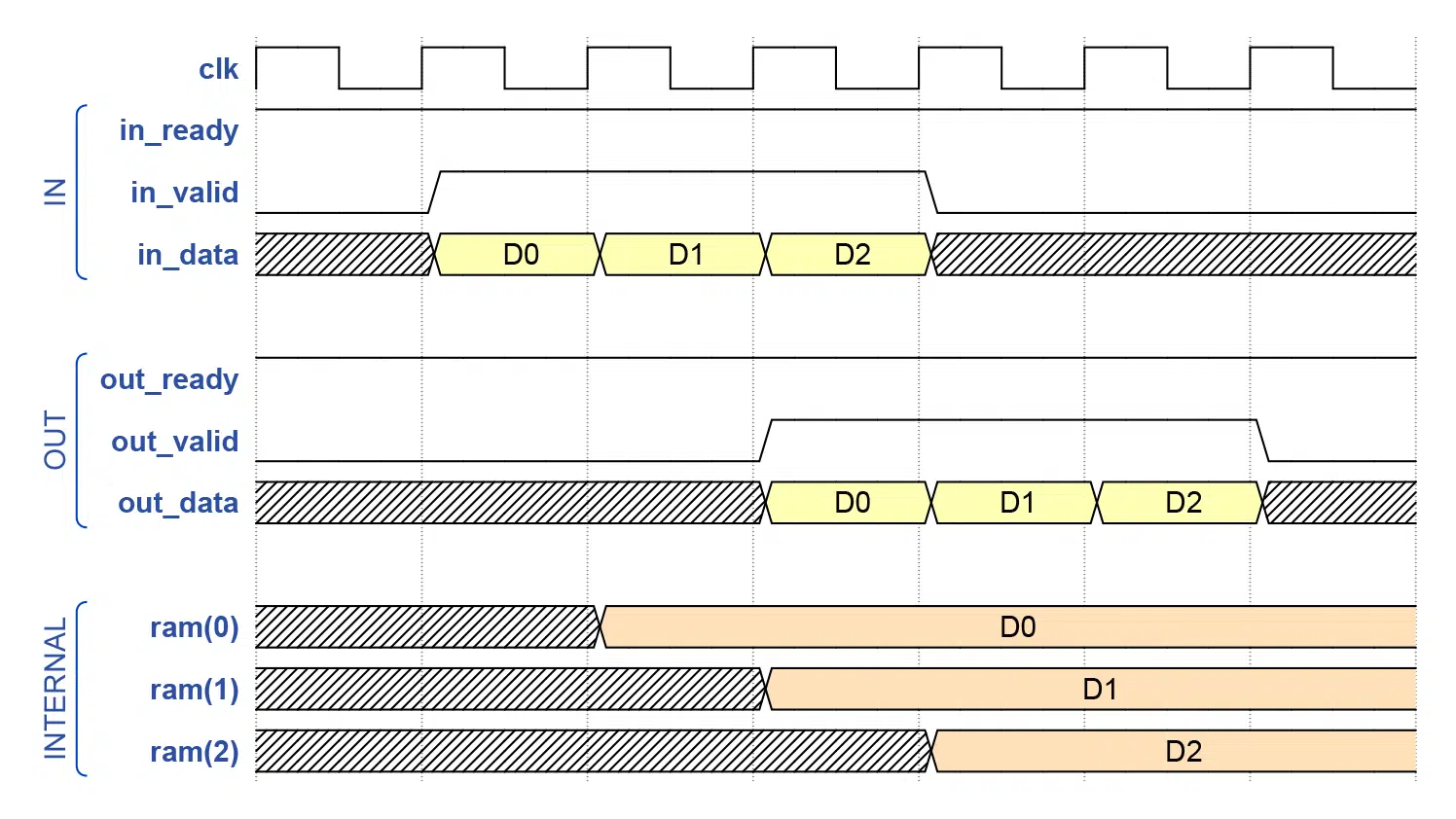
Consider the waveform below. Initially, the FIFO is empty, as denoted by the count signal being 0. Then, a write occurs on the third clock cycle. RAM slot 0 is updated in the next clock cycle, but it takes an additional cycle before the data appears on the out_data output. The purpose of the or count_p1 = 0 statement is to make sure that out_valid remains '0' (circled in red) while the value propagates through the RAM.

The last If-statement guards against another corner case. We have just talked about how to handle the special case of write-on-empty by checking the current and previous FIFO fill levels. But what happens if and we perform a simultaneous read and write when count already is 1?
The waveform below shows such a situation. Initially, there is one data item D0 present in the FIFO. It has been there for a while, so both count and count_p1 are 0. Then a simultaneous read and write comes along in the third clock cycle. One item leaves the FIFO and a new one enters it, rendering the counters unchanged.

At the moment of reading and writing, there is no next value in the RAM ready to be output, as there would have been if the fill level was higher than one. We have to wait for two clock cycles before the input value appears on the output. Without any additional information, it would be impossible to detect this corner case, and the value of out_valid at the following clock cycle (marked as solid red) would be erroneously set to '1'.
That’s why we need the read_while_write_p1 signal. It detects that there has been a simultaneous read and write, and we can take this into account by setting out_valid to '0' in that clock cycle.
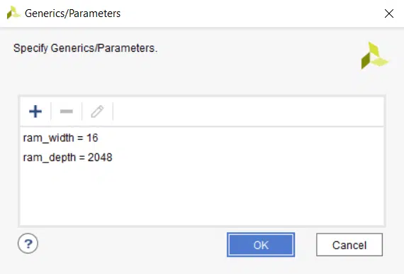
Synthesizing in Vivado
To implement the design as a stand-alone module in Xilinx Vivado we first have to give values to the generic inputs. This can be achieved in Vivado by using the Settings → General → Generics/Parameters menu, as shown in the image below.
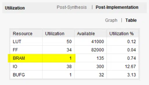
The generic values have been chosen to match the RAMB36E1 primitive in the Xilinx Zynq architecture which is the target device. Post-implementation resource usage is shown in the image below. The AXI FIFO uses one block RAM and a small number of LUTs and flip-flops.
AXI is more than ready/valid
AXI stands for Advanced eXtensible Interface, it’s part of ARM’s Advanced Microcontroller Bus Architecture (AMBA) standard. The AXI standard is a lot more than the read/valid handshake. If you want to know more about AXI I recommend these resources for further reading:
Need the Questa/ModelSim project files?
Let me send you a Zip with everything you need to get started in 30 seconds
Tested on Windows and Linux Loading Gif..
Hello Jonas,
I am very interested in this article and about your blog vhdl.
I am an engineering student and I would like to create a circular fifo buffer to store data in registers or ram
I use a test and development card “Zedboard” with a Zynq.
Your fifo interests me, however I do not know enough the AXI bus to create a customisable IP to integrate it into an acquisition chain.
My project is to have a circular fifo, which retrieves data from a random counter (simulated data) and writes them in registers that the fpga will read
Have you already implemented a custom ip AXI4 (Lite) of this fifo ?
Sorry for my basic english
Thanks a lot
Hi Raphaël,
You can read more about implementing a circular buffer FIFO using block RAM in the article How to create a ring buffer FIFO in VHDL. I have synthesized both this FIFO and the one in the previously mentioned article for the Zynq architecture. It works, just download the example project by using the Need the ModelSim project files? form above the comment section. There, you will find an example instantiation of the AXI FIFO in the testbench file. You are free to use the FIFO in your project.
– Jonas
Hi Jonas,
Thanks a lot for you response
However as I told you I am not an expert in AXI interface and I would like to know what is meant by an example of instantiation ? What should I use in my AXI top level ?
Do you have a tutorial to recommend me on building a custom AXI IP ?
That I can understand how this is done from A to Z.
Thanks
Hi Raphaël,
This FIFO uses the AXI style ready/value handshake, it doesn’t implement the whole AXI or AXI Lite protocol. The FIFO can be used on one AXI channel, or independently of AXI because it’s a convenient handshaking mechanism.
I think you just have to search the internet because at this time I don’t have any A to Z AXI tutorial. Perhaps you should look at the documentation for whatever AXI endpoint you wish to communicate with.
Best of luck.
– Jonas
Hi Jonas,
I did a try on the tutorial above and implement it in a cool project (driving RGB adressable LED 5050 type for color control). There is something that I don’t understant in the behavior in the axi fifo.
The “in_data” value is updated to “X” at the read process and the value at the last address is updated to “X” instead of the last data written, regardless of the “in_valid” state.
Keep doing you great tutorail!
Thanks!
Hello Jean-Yves,
Sorry about the late reply, and it’s great to hear that you used the code in a cool project!
If I understand correctly, you are wondering why we are writing to
ram(head)regardless of thein_validsignal. We can see from the process below that this is happening on every clock cycle.PROC_RAM : process(clk) begin if rising_edge(clk) then ram(head) <= in_data; out_data <= ram(next_index(tail, out_ready, out_valid_i)); end if; end process;It’s because if we use a condition like
in_valid = '1'it won’t synthesize into block RAM. In most architectures, there can be no logic on the input port of the block RAM. The optional write enable must come from a register, and that would be too slow for us because we want to be able to write on every clock cycle.Instead, we write to
ram(head)continuously and regard this RAM slot as transient until theheadaddress is incremented.Block RAM can be tricky to work with; it requires different thinking than registers because the rules are not as flexible.
Jean-Yves Bourque
dim. 10 janv. 18:18 (il y a 14 heures)
À Jonas

Thanks Jonas,
Just to give you some news.
After running analysis and synthesis with Intel-Quartus with a MAX-10 device, here is the result:
1 – A sync Ram bloc was used. (note that the WE signal is always enabled, stock at 1).
2 – It works perfectly, as you described in your tutorial.
3 – Definitively hard to implement and control correctly (data at right address).
4 – It holds the audio power meter and the color mixer value.
5 – Waiting for the MSGEQ7 devices to implement the ADC side and complete the project.
Salutations,
Hello Jonas
great tutorial!
Since we do not use wr enable signal, we write the memory in each clk cycle, in that case it is necessary to keep the value of the data in the “in_data” port, that is, the driver should not change the data until “in_ready = 1 “
Hello!
I implement dual port ram. I work in ISE. It gives I should use shared variable for declaration the signal. I declared it as signal as you did. Could you please explain why shared variable should be used in a ram signal declaration?
Hello, Anna. I can’t think of a reason for that error message. I don’t have enough information about the design. Perhaps you would like to join the private Facebook group where you can discuss such problems with thousands of other VHDL users?
https://web.facebook.com/groups/vhdlwhiz
You have made it look as simple as it can look, however I am still amazed that someone would think the AXI standard is “cool” when you look at the amount of code you had to write to implement a simple FIFO. I find that the amount of glue logic is often proportional to the number of bugs found in simulation (though I am sure this code is clean). Finding bugs in most AXI implementations is very difficult because there are a lot of corner cases. I wish the vendors had settled on a simpler standard.
None the less, your article is very good and your coding is solid and I enjoyed the article.
I like the ready/valid handshake, but we probably have to use a different term than “simple” to describe the full AXI protocol. 😅
Thank you for commenting!
Hi Jonas,
Thanks for your code, it’s well written. My project requires such an AXI FIFO. I am interested in your project. If we want to use width and depth that aren’t powers of 2, how do we do that? In this case, could the FIFO be assigned to RAM?
You can assign a value to ram_depth that’s not a power of 2, but then the rest of the block RAM primitive will be wasted because other logic can’t use the remaining space. Sometimes, that’s what you want, but most often, bigger is better.
You’ve got to check the width and depth of the BRAM primitives on your target FPGA to find optimal values.
I see two issues in the above code example. First, most modules that use the AXI-Stream interface expect that it includes tkeep and tlast signals. Without these signals, the FIFO cannot be connected to such modules. Second, for Vivado to infer the AXI-Stream interface, the port names should follow some naming conventions. With the port names used in the above example, Vivado does not infer AXI-Stream interfaces.
Sure, I agree with you.
I don’t want to update the code from this article because it’s referenced from many places, and the images show the old signal names, but I might make a new blog post about it.
You can make a wrapper VHDL file for the FIFO to add the new signals and change the names.
Hi,
I am a little confused about the update of the ‘tail’.
It is updated in PROC_RAM and also in the PROC_TAIL.
How does that work?