I’ve noticed that many of the gadgets that I’ve bought the last couple of years have shifted away from LED blinking to led breathing. Most electronic gizmos contain a status LED whose behavior gives away indications of what’s going on inside of the device.
My electric toothbrush flashes an LED when it’s time to recharge it, and my mobile phone uses the LED to call my attention for a wide variety of reasons. But the LEDs aren’t blinking as they did in the old days. It’s more like an analog pulsing effect with continuous varying intensity.
The Gif animation below shows my Logitech mouse using this effect to indicate that it’s charging the battery. I call this effect breathing LED because the light intensity pattern is similar in speed and acceleration to the human breathing cycle. It looks so natural because the illumination cycle follows a sine wave pattern.

This article is a continuation of last week’s blog post about pulse-width modulation (PWM). Today, we are going to use the PWM module, the sawtooth counter, and the reset module that we created in the previous tutorial. Click the link below to read the article about PWM!
How to create a PWM controller in VHDL
Storing sine wave values in block RAM
While it’s possible to generate a sine wave using digital signal processing (DSP) primitives in the FPGA, a more straightforward way is storing the sample points in block RAM. Instead of computing the values during run-time, we calculate a series of sine values during synthesis and create a read-only memory (ROM) to store them in.
Consider the minimal example below, which shows how to store a full sine wave in a 3×3 bits ROM. Both the address input and the data output are three bits wide, meaning that they can represent an integer value on the range from 0 to 7. We can store eight sine values in the ROM, and the resolution of the data is also 0 to 7.
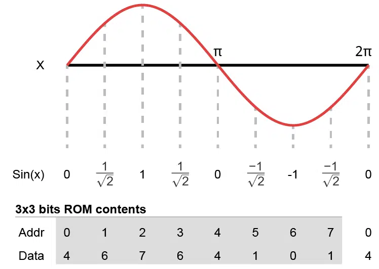
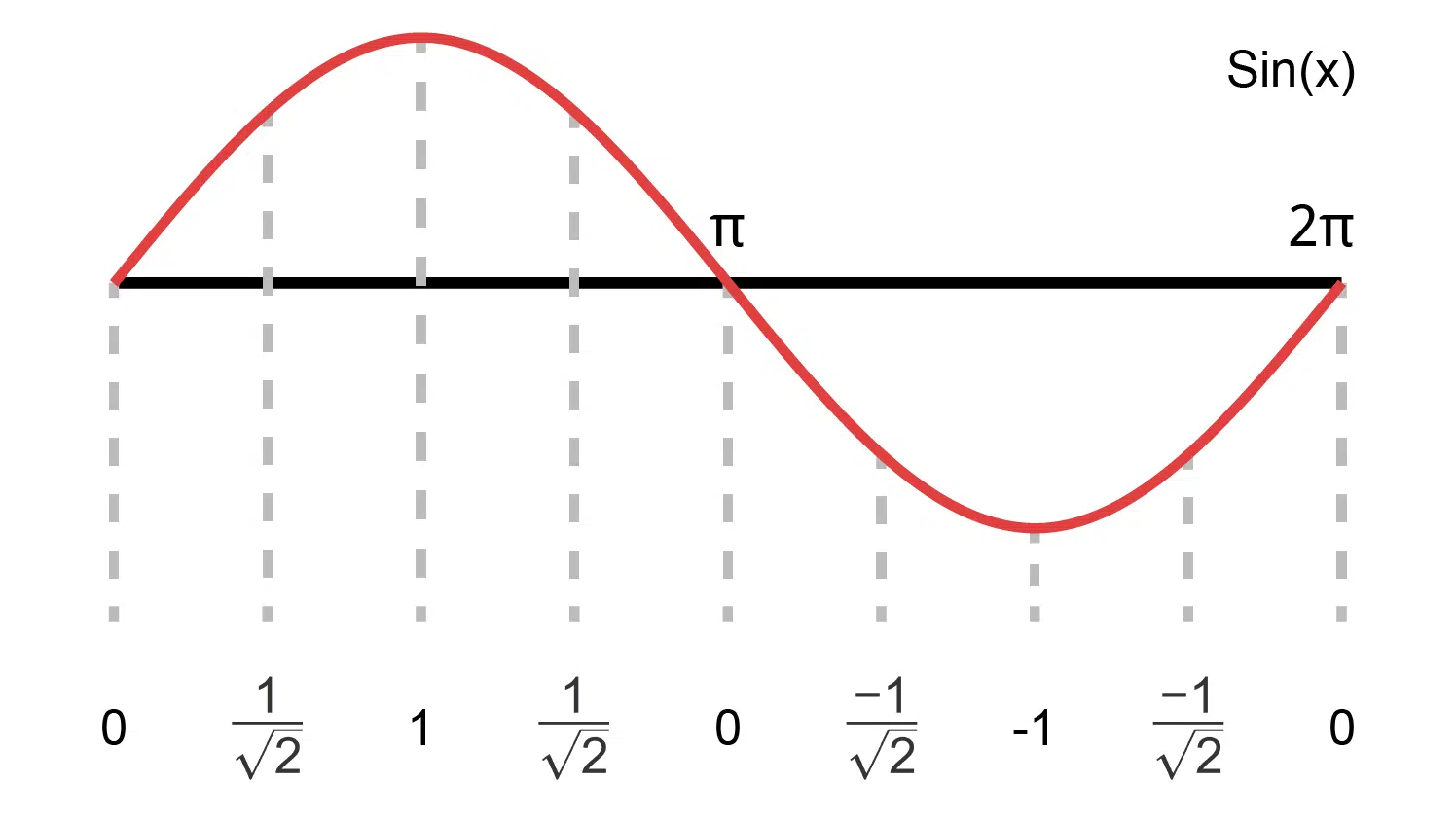
The trigonometric sine function produces a number on the range [-1, 1] for any angle input, x. Also, the cycle repeats when x ≥ 2π. Therefore, it’s sufficient to store only the sine values from zero and up to, but not including 2π. The sine value for 2π is the same as the sine for zero. The illustration above shows this concept. We are storing sine values from zero to \frac{7\pi}{4}, which is the last evenly spaces step before the full 2π circle.
Digital logic cannot represent real values, like the angle or sine values, with infinite precision. That’s the case in any computer system. Even when using double-precision floating-point numbers, it’s just an approximation. That’s how binary numbers work, and our sine ROM is not different.
To get the most out of the available data bits, we add an offset and a scale to the sine values when we calculate the ROM content. The lowest possible sine value of -1 maps to the data value 0, while the highest possible sine value of 1 translates into 2^{\mathit{data\_bits}-1}, as shown by the formula below.
\mathit{data} = \mathit{Round}\left(\frac{(1 + \sin \mathit{addr}) * (2^\mathit{data\_bits} - 1)}{2}\right)To translate a ROM address into an angle, x, we can use the following formula:
x = \frac{\mathit{addr} * 2\pi}{2^\mathit{addr\_bits}}Of course, this method doesn’t give you a universal angle to sine value converter. If that’s what you want, you will have to use additional logic or DSP primitives to scale the address input and the data output. But for many applications, a sine wave represented as an unsigned integer is good enough. And as we shall see in the next section, it’s exactly what we need for our example LED pulsing project.
Sine ROM module
The sine ROM module presented in this article will infer block RAM on most FPGA architectures. Consider matching the width and depth generics to the memory primitives of your target FPGA. That will give you the best resource utilization. You can always refer to the example Lattice project if you’re unsure of how to use the sine ROM for a real FPGA project.
Leave your email in the form below to download the VHDL files and ModelSim / iCEcube2 projects!
Need the Questa/ModelSim project files?
Let me send you a Zip with everything you need to get started in 30 seconds
Tested on Windows and Linux Loading Gif.. 
The entity
The code below shows the entity of the sine ROM module. It contains two generic inputs that let you specify the width and depth of the inferred block RAM. I’m using range specifiers on the constants to prevent unintentional integer overflow. More on that later in this article.
entity sine_rom is
  generic (
    addr_bits : integer range 1 to 30;
    data_bits : integer range 1 to 31
  );
  port (
    clk : in std_logic;
    addr : in unsigned(addr_bits - 1 downto 0);
    data : out unsigned(data_bits - 1 downto 0)
  );
end sine_rom;
The port declaration has a clock input, but no reset because RAM primitives can’t have reset. The addr input is where we assign the scaled angle (x) value, and the data output is where the scaled sine value will appear.
Type declarations
At the top of the VHDL file’s declarative region, we declare a type and a subtype for our ROM storage object. The addr_range subtype is an integer range equal to the number of slots in our RAM, and the rom_type describes a 2D array that will store all of the sine values.
subtype addr_range is integer range 0 to 2**addr_bits - 1;
type rom_type is array (addr_range) of unsigned(data_bits - 1 downto 0);
However, we are not going to declare the storage signal just yet. First, we need to define the function that will produce the sine values, which we can use to turn the RAM into a ROM. We have to declared it above the signal declaration so that we can use the function to assign an initial value to the ROM storage signal.
Note that we are using the addr_bits generic as a base for defining addr_range. That’s the reason why I had to specify a max value of 30 for addr_bits. Because for larger values, the 2**addr_bits - 1 calculation will overflow. VHDL integers are 32-bits long, although that’s about to change with VHDL-2019, which used 64-bit integers. But for now, we have to live with this limitation when using integers in VHDL until the tools start supporting VHDL-2019.
Function for generating sine values
The code below shows the init_rom function that generates the sine values. It returns a rom_type object, which is why we have to declare the type first, then the function, and finally, the ROM constant. They depend on each other in that exact order.
function init_rom return rom_type is
  variable rom_v : rom_type;
  variable angle : real;
  variable sin_scaled : real;
begin

  for i in addr_range loop

    angle := real(i) * ((2.0 * MATH_PI) / 2.0**addr_bits);
    sin_scaled := (1.0 + sin(angle)) * (2.0**data_bits - 1.0) / 2.0;
    rom_v(i) := to_unsigned(integer(round(sin_scaled)), data_bits);

  end loop;

  return rom_v;
end init_rom;
The function uses a few convenience variables, including rom_v, a local copy of the array that we fill with sine values. Inside the subprogram, we use a for-loop to iterate over the address range, and for each ROM slot, we calculate the sine value using the formulas that I described earlier. And in the end, we return the rom_v variable that by now contains all the sine samples.
The integer conversion on the last line in the for-loop is the reason why I had to restrict the data_bits generic to 31 bits. It will overflow for any larger bit lengths.
constant rom : rom_type := init_rom;
Below the init_rom function definition, we go on to declare the rom object as a constant. A ROM is simply a RAM that you never write to, so that’s perfectly fine. And now it’s time to use our function. We call init_rom to generate the initial values, as shown in the code above.
The ROM process
The only logic in the sine ROM file is the rather simple process that’s listed below. It describes a block RAM with a single read port.
ROM_PROC : process(clk)
begin
  if rising_edge(clk) then
    data <= rom(to_integer(addr));
  end if;
end process;
Top module
This design is a continuation of the PWM project that I presented in my previous blog post. It has a reset module, a PWM generator module, and a free-running clock cycle counter (sawtooth counter) module. Refer to last week’s article to see how these modules work.
The diagram below shows the connections between the submodules in the top module.
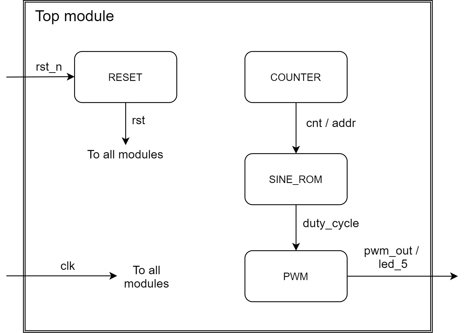
The code below shows the declarative region of the top VHDL file. In last week’s PWM design, the duty_cycle object was an alias for the MSBs of the cnt counter. But that wouldn’t work now because the output from the sine ROM will control the duty cycle, so I’ve replaced it with an actual signal. Moreover, I’ve created a new alias with the name addr that is the MSBs of the counter. We will use it as the address input for the ROM.
signal rst : std_logic;
signal cnt : unsigned(cnt_bits - 1 downto 0);
signal pwm_out : std_logic;
signal duty_cycle : unsigned(pwm_bits - 1 downto 0);

-- Use MSBs of counter for sine ROM address input
alias addr is cnt(cnt'high downto cnt'length - pwm_bits);
You can see how to instantiate our new sine ROM in the top module in the listing below. We set the RAM’s width and depth to follow the length of the PWM module’s internal counter. The data output from the ROM controls the duty_cycle input to the PWM module. The value on the duty_cycle signal will portray a sine wave pattern when we read out the RAM slots one after the other.
SINE_ROM : entity work.sine_rom(rtl)
  generic map (
    data_bits => pwm_bits,
    addr_bits => pwm_bits
  )
  port map (
    clk => clk,
    addr => addr,
    data => duty_cycle
  );
Simulating the sine wave ROM
The image below shows the waveform of the top module simulation in ModelSim. I’ve changed the presentation of the unsigned duty_cycle signal to an analog format so that we can observe the sine wave.
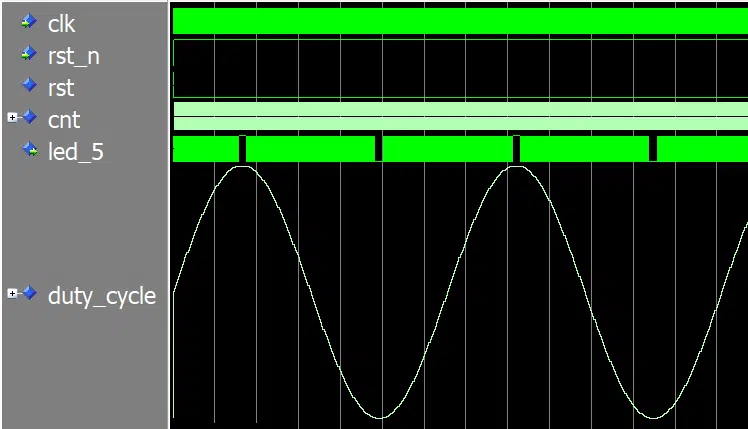
It is the led_5 top-level output that carries the PWM signal, which controls the external LED. We can see that the output is changing rapidly when the duty cycle is rising or falling. But when the duty cycle is at the top of the sine wave, led_5 is a steady ‘1’. When the wave is at the bottom of the slope, the output stays briefly at ‘0’.
Want to try it out on your home computer? Enter your email address in the form below to receive the VHDL files and the ModelSim and iCEcube2 projects!
Need the Questa/ModelSim project files?
Let me send you a Zip with everything you need to get started in 30 seconds
Tested on Windows and Linux Loading Gif..
Implementing LED breathing on the FPGA
I used the Lattice iCEcube2 software to implement the design on the iCEstick FPGA board. Use the form above to download the project and try it out on your board if you own an iCEstick!
The listing below shows the resource usage, as reported by the Synplify Pro software that comes with iCEcube2. It shows that the design uses one block RAM primitive. That’s our sine ROM.
Resource Usage Report for led_breathing

Mapping to part: ice40hx1ktq144
Cell usage:
GND             4 uses
SB_CARRY        31 uses
SB_DFF          5 uses
SB_DFFSR        39 uses
SB_GB           1 use
SB_RAM256x16    1 use
VCC             4 uses
SB_LUT4         65 uses

I/O ports: 7
I/O primitives: 7
SB_GB_IO       1 use
SB_IO          6 uses

I/O Register bits:                  0
Register bits not including I/Os:   44 (3%)

RAM/ROM usage summary
Block Rams : 1 of 16 (6%)

Total load per clock:
   led_breathing|clk: 1

@S |Mapping Summary:
Total  LUTs: 65 (5%)
After routing the design in iCEcube2, you will find the .bin file in the led_breathing_Implmnt\sbt\outputs\bitmap folder inside of the Lattice_iCEcube2_proj project directory.
You can use the Lattice Diamond Programmer Standalone software to program the FPGA, as shown in the iCEstick user manual. That’s what I did, and the Gif animation below shows the result. The light intensity of the LED oscillates with a sine wave pattern. It looks very natural, and the LED appears to be “breathing” if you put some imagination into it.
Final thoughts
Using block RAM for storing precalculated sine values is pretty straightforward. But there are a few limitations that make this method suitable only for sine waves with limited X and Y resolutions.
The first reason that comes to mind is the 32-bit limit for integer values that I discussed earlier. I’m sure you can overcome this problem by calculating the sine value more cleverly, but that’s not all.
For every bit you extend the ROM address with, you are doubling the RAM usage. If you need high precision on the X-axis, there may not be enough RAM, even on a larger FPGA.
If the number of bits used for the Y-axis sine values exceeds the native RAM depth, the synthesis tool will use additional RAMs or LUTs to implement the ROM. It will eat up more of your resource budget as you increase the Y precision.
In theory, we only need to store one quadrant of the sine wave. Therefore, you could get away with a quarter of the RAM usage if you used a finite-state machine (FSM) to control the ROM readout. It would have to invert the sine quadrant in for all four permutations of the X and Y axes. Then, you could build a full sine wave from the single quadrant stored in block RAM.
Unfortunately, it’s difficult to get all four segments to join smoothly. Two equal samples in the joints at the top and bottom of the sine wave distorts the data by creating flat spots on the sine wave. Introducing noise defeats the purpose of storing only the quadrant to improve the precision of the sine wave.


Nice writeup! I really like this idea of using Block RAM as a lookup table, because there is virtually no additional logic resources needed in the FPGA. Of course, you do need to have a sufficient number of Block RAM, but even using just a single Block RAM will usually give you sufficient precision in both X and Y directions.
You mention stitching together multiple quadrants and the problem of avoiding distortion. I saw in another project (the YM2151 sound synthesizer) a neat little trick: Offset the x-coordinate by half a unit, i.e. replace (in line 9) the part
with
. This actually makes the stitching together somewhat easier because there are no longer any awkward edge cases to have to consider.
Interesting! I’m going to write that down. Maybe there will be a follow-up article. ?
This article helps out a lot!
Could you please tell me what would be the formula or way to determine the period/frequency of the sine signal? Would it be possible to change it and how, ie. what is it dependent on exactly? Thank you!
Assuming that you read one sample per clock cycle and go through all addresses continuously, the frequency is a function of the number of address bits and the FPGA clock speed: Freq = clk_hz / 2^addr_bits. For example, if the system clock is 100 MHz and you set
addr_bitsto 12, the frequency will be: 100e6 / 2^12 ≈ 24415 Hz.Hi, This article is very helpful.
Please tell me, if I want to generate the chirp signal (LFM) from this code, by changing the frequency linearly after some delay, how will I solve this in test bench vhdl code.
Thanks..
Hello, you have to change the formula in the
init_romfunction to generate your desired waveform.please tell me the which variable is used in the init_rom to change the frequency linearly.
To generate the different single frequency of wave, I am changing cnt_bits in the test bench.
How i can generate the sweep of changing frequencies.
Hello Jonas,
thanks for this great post.
I did not understand why you are declaring such an amount of address bits:
in sine_rom.vhd when changing it later in led_breathing.vhd to:
Is it to correctly define the ROM, or just to be flexible later on?
At synthesis I also have eight address bits, haven’t I?
The ranges on the generic port constants prevent the user from assigning values that don’t work. They are max/min values.
When I wrote this code, I identified the max
addr_bitsvalue that doesn’t result in overflow in theinit_rom()calculations.Yes, you will get eight bits after synthesis if you assign 8 to
addr_bitswhen instantiating.