There are many ways to create a shift register in VHDL, though not all of them are equal. You can dramatically reduce the number of consumed resources by choosing the right shift register implementation for your needs and FPGA architecture.
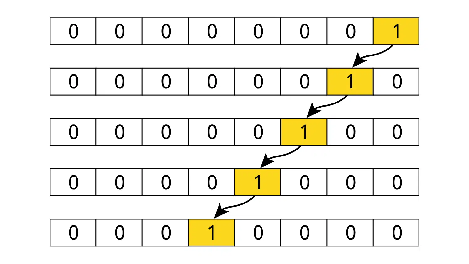
A shift register implements a FIFO of fixed length. Every time a new element enters the queue, it shifts the existing ones one place further away from the input. To understand the basics of the shift register, I recommend viewing the VHDL tutorial about the std_logic_vector.
This article will only consider the shift register, even though there exist data structures that use fewer resources for larger FIFOs. Read about how to create a ring buffer FIFO in block RAM to learn about such a solution that’s not a shift register.
While any shift register is suitable for creating generic, smaller buffers, there are methods of efficiently creating larger ones. Many FPGAs have logic elements that can double as specialized shift register primitives. You can improve performance in magnitudes by being mindful of how you write your VHDL code.
The 1-bit shift register with generic depth
Let’s first have a look at different methods of creating a one-bit shift register. The input and output of this shift register is a single bit, a std_logic value. The depth is configurable through a generic constant.
We will use the entity declaration shown below for all of the following examples involving one-bit shift registers. To keep it simple, we’re going to use the same entity for multiple architectures, even though the rst and enable inputs are unused by some of them.
entity shift_reg_1_width is
  generic (
    sr_depth : integer
  );
  port (
    clk : in std_logic;

    rst : in std_logic; -- Optional
    enable : in std_logic; -- Optional

    sr_in : in std_logic;
    sr_out : out std_logic
  );
end;
The three implementations that follow will synthesize into the same logic. These are the resources consumed for Xilinx, Intel (Altera), and Lattice FPGAs with the sr_depth generic set to 128.
| Xilinx Vivado (Zynq): | 4 LUTs (LUTRAM) + 2 FFs |
| Intel Quartus II (Cyclone V) | 11 ALMs + 1 BRAM |
| Lattice IceCube2 (iCE40) | 128 FFs |
Even though the shift register should require 128 flip-flops (FFs), we see that the resource usage reported by Vivado and Quartus is far less. Instead of using expensive FFs, the synthesis tools have used special built-in features of the logic blocks.
Lookup tables (LUTs) used in such a way are counted as “LUTRAM” in the Vivado resource usage report. In the Intel FPGA, adaptive logic modules (ALMs) and one block RAM (BRAM) is used instead of flip-flops. Intel uses a technology that they call ALTSHIFT_TAPS for implementing RAM-based shift registers.
The Lattice iCE40 FPGA, which I used in this example, doesn’t have an alternative option for packing 1-bit shift register, so it’s implemented entirely in 128 FFs. However, we shall see later in this article that the Lattice device can pack wider shift registers into block RAM.
Need the Questa/ModelSim project files?
Let me send you a Zip with everything you need to get started in 30 seconds
Tested on Windows and Linux Loading Gif.. 
Slicing the vector
The most straightforward way to create a shift register is to use vector slicing. Insert the new element at one end of the vector, while simultaneously shifting all of the others one place closer to the output side. Put the code in a clocked process and tap the last bit in the vector, and you have your shift register.
architecture slicing of shift_reg_1_width is

  signal sr : std_logic_vector(sr_depth - 2 downto 0);

begin

  process(clk)
  begin
    if rising_edge(clk) then

      sr <= sr(sr'high - 1 downto sr'low) & sr_in;
      sr_out <= sr(sr'high);

    end if;
  end process;

end architecture slicing;
Using a for-loop
Just like vector slicing, the for-loop also works in all revisions of the VHDL language. This approach requires an additional line of code to assign the input to the vector. Remember that every iteration of the for-loop is executed in zero time in RTL code because there’s no wait-statement inside of it. Therefore, this code is logically equivalent to the previous example.
architecture for_loop of shift_reg_1_width is

  signal sr : std_logic_vector(sr_depth - 2 downto 0);

begin

  process(clk)
  begin
    if rising_edge(clk) then

      for i in sr'high downto sr'low + 1 loop
        sr(i) <= sr(i - 1);
      end loop;

      sr(sr'low) <= sr_in;
      sr_out <= sr(sr'high);

    end if;
  end process;

end architecture for_loop;
Using the shift_left function
While the previous examples work for vectors as well as arrays of any kind, using the shift_left function only works with bit vectors. The definition of the shift_left function and it’s complementary shift_right function appears in the ieee.numeric_std package. It requires an unsigned vector as the first parameter, and that’s why it’s not suitable for arrays of arbitrary data types.
architecture ieee_shift_left of shift_reg_1_width is

  signal sr : unsigned(sr_depth - 2 downto 0);

begin

  process(clk)
  begin
    if rising_edge(clk) then

      sr <= shift_left(sr, 1);
      sr(sr'low) <= sr_in;
      sr_out <= sr(sr'high);

    end if;
  end process;

end architecture ieee_shift_left;
Enable input
Most FPGA architectures have flip-flops with an optional enable (E) or clock enable (CE) input. This functionality can’t be utilized by any other logic when you are using it for the shift register. Thus, the additional enable input won’t consume extra resources.
Wrap the code that’s responsible for shifting with an if enable = '1' then statement. Then, input and output from the shift register will still occur on the rising edge of the clock, but only when the enable input is asserted.
The code below shows the previous example with the enable input added to the implementation.
architecture with_enable of shift_reg_1_width is

  signal sr : unsigned(sr_depth - 2 downto 0);

begin

  process(clk)
  begin
    if rising_edge(clk) then

      if enable = '1' then
        sr <= shift_left(sr, 1);
        sr(sr'low) <= sr_in;
        sr_out <= sr(sr'high);
      end if;

    end if;
  end process;

end architecture with_enable;
The drawback of having a reset value
You should be cautious about adding reset values to the shift register vector or output. The problem is that it prevents the synthesis tool from packing the shift register into LUTs or BRAM. Consider the example below, which is the same as the first one in this article, but with synchronous reset added.
architecture slicing_with_rst of shift_reg_1_width is

  signal sr : std_logic_vector(sr_depth - 2 downto 0);

begin

  process(clk)
  begin
    if rising_edge(clk) then
      if rst = '1' then
        sr <= (others => '0');
        sr_out <= '0';

      else
        sr <= sr(sr'high - 1 downto sr'low) & sr_in;
        sr_out <= sr(sr'high);

      end if;
    end if;
  end process;

end architecture slicing_with_rst;
Now, the resource usage for both Xilinx and Intel FPGAs has jumped to 128 FFs. For Intel FPGAs, it makes the most sense to measure resource usage in ALMs, but they contain the same number of FFs as the other FPGAs used.
| Xilinx Vivado (Zynq) | 128 FFs |
| Intel Quartus II (Cyclone V) | 33 ALMs |
| Lattice IceCube2 (iCE40) | 128 FFs |
The synchronous reset has forced the synthesis tool to implement the shift register entirely in FFs. Therefore, you should ask yourself if you need to be able to reset the entire shift register at once.
Using a counter to reset the output
After reset, everything that’s in the shift register is invalidated. Usually, you don’t care what the invalid data is, the purpose of the reset is to avoid passing it on to downstream modules. An alternative to resetting the entire shift register is to monitor where the valid data starts inside of it.
While invalid data is at the output, you forward your reset value. Then, when valid data reaches the output, you start sampling the real output from the shift register. As long as you don’t tap the shift register other than at the output, the behavior will be indistinguishable from true synchronous reset.
The code below uses a counter signal to implement synchronous reset of the shift register output.
architecture rst_counter of shift_reg_1_width is

  signal sr : std_logic_vector(sr_depth - 2 downto 0);
  signal rst_counter : integer range 0 to sr_depth - 1;

begin

  process(clk)
  begin
    if rising_edge(clk) then
      if rst = '1' then
        rst_counter <= 0;
        sr_out <= '0';

      else

        sr <= sr(sr'high - 1 downto sr'low) & sr_in;

        if rst_counter = sr_depth - 1 then
          sr_out <= sr(sr'high);
        else
          rst_counter <= rst_counter + 1;
          sr_out <= '0';
        end if;

      end if;
    end if;
  end process;

end architecture rst_counter;
As we can see from the resource usage below, Xilinx has gone back to using LUTRAM and Intel to ALMs and a single BRAM primitive. The implementation uses a bit more logic for the new counter, but overall the saving is substantial. The exception is the Lattice device, which consumes more than before because it doesn’t have primitives for optimizing this kind of shift register.
| Xilinx Vivado (Zynq) | 12 LUTs (4 LUTRAM) + 9 FFs |
| Intel Quartus II (Cyclone V) | 17 ALMs + 1 BRAM |
| Lattice IceCube2 (iCE40) | 18 LUTs + 135 FFs |
Shift register with generic depth and width
Let’s proceed to look at an implementation of a shift register with configurable data width as well. The code below shows the entity used in the following examples. It has two generic inputs, one for setting the depth and one for the width of the data elements.
entity shift_reg_generic_width is
  generic (
    sr_depth : integer;
    sr_width : integer
  );
  port (
    clk : in std_logic;
    rst : in std_logic; -- Optional

    sr_in : in std_logic_vector(sr_width - 1 downto 0);
    sr_out : out std_logic_vector(sr_width - 1 downto 0)
  );
end;
In the examples below, we will assign 128 to the sr_depth generic and 16 to the sr_width generic.
Without reset
In the code below, we have converted the slicing example without reset to have configurable width as well as depth. We synthesize it with an input width of 16, meaning that it can store 16 times as many bits as the first example in this article. Let’s see if the resource usage is multiplied by 16 too.
architecture slicing of shift_reg_generic_width is

  type sr_type is array (sr_depth - 2 downto 0)
    of std_logic_vector(sr_width - 1 downto 0);
  signal sr : sr_type;

begin

  process(clk)
  begin
    if rising_edge(clk) then

      sr <= sr(sr'high - 1 downto sr'low) & sr_in;
      sr_out <= sr(sr'high);

    end if;
  end process;

end architecture slicing;
The resource utilization is listed below. Xilinx has gone from 4 to 64 LUTs, and from 2 to 32 FFs, 16 times the resources exactly. Intel, on the other hand, has risen from 11 ALMs to 20 ALMs, still using one BRAM. The reason for the modest increase is because the BRAM can accommodate far more data than we are asking for in the first place, it just needs a bit more control logic.
| Xilinx Vivado (Zynq) | 64 LUTs (LUTRAM) + 32 FFs |
| Intel Quartus II (Cyclone V) | 20 ALMs + 1 BRAM |
| Lattice IceCube2 (iCE40) | 18 LUTs + 1 BRAM + 25 FFs |
Finally, the Lattice FPGA has managed to pack the wider shift register into block RAM. Its resource usage is now on par with Xilinx and Intel.
With a smart reset counter
The final example in this article is a shift register with generic width and depth, using synchronous reset. The code below shows the implementation which uses the reset counter that we discussed earlier in this article.
architecture counter_rst of shift_reg_generic_width is

  type sr_type is array (sr_depth - 2 downto 0)
    of std_logic_vector(sr_width - 1 downto 0);
  signal sr : sr_type;

signal rst_counter : integer range 0 to sr_depth - 1;

begin

  process(clk)
  begin
    if rising_edge(clk) then
      if rst = '1' then
        rst_counter <= 0;
        sr_out <= (others => '0');

      else

        sr <= sr(sr'high - 1 downto sr'low) & sr_in;

        if rst_counter = sr_depth - 1 then
          sr_out <= sr(sr'high);
        else
          rst_counter <= rst_counter + 1;
          sr_out <= (others => '0');
        end if;

      end if;
    end if;
  end process;

end architecture counter_rst;
We can see from the listing below that the Xilinx FPGA needs eight additional regular LUTs and seven FFs for implementing the counter reset. Intel Quartus II still somehow reports the same resource usage as without reset. The Lattice FPGA consumes 24 more LUTs and 31 more FFs for implementing the counter, but the shift register still fits in one BRAM.
| Xilinx Vivado (Zynq) | 72 LUTs (64 LUTRAM) + 39 FFs |
| Intel Quartus II (Cyclone V) | 20 ALMs + 1 BRAM |
| Lattice IceCube2 (iCE40) | 42 FFs + 1 BRAM + 56 FFs |
Try out all the different shift registers in ModelSim for free. Use the form below to download the ModelSim project with all the code. Have it up and running within minutes!
Need the Questa/ModelSim project files?
Let me send you a Zip with everything you need to get started in 30 seconds
Tested on Windows and Linux Loading Gif..
Controlling the RAM usage with synthesis attributes
The synthesis tools will try to use the FPGA primitives that give the highest device utilization. The cheapest resource is BRAM, then comes distributed RAM or LUTRAM, and finally, FFs which are the most valuable.
But you can override the automatic choice by using a synthesis attribute, also known as a pragma or compiler directive. The different FPGA vendors have their own sets of VHDL attributes. To specify a desired primitive type, you define the attribute in the architecture region of the VHDL file, referencing your shift register array or vector by name.
Xilinx Vivado
The Xilinx UG901 user guide lists all synthesis attributes that are recognized by Vivado. The shreg_extract attribute and the srl_style attribute are the ones that control shift register synthesis.
Setting the shreg_extract attribute to "no" disables all shift register optimization. This setting acts like a master switch, overriding other SRL synthesis settings. You can also assign "yes" to shreg_extract, but this is the default setting anyway.
attribute shreg_extract : string;
-- attribute shreg_extract of sr : signal is "yes";
attribute shreg_extract of sr : signal is "no";
Remember to replace sr with the name of your shift register signal.
The next attribute of interest is srl_style. It’s a request to the synthesis tool to implement the shift register in a specific type of primitive. Note that this is not a magic pill. For example, you can’t force the synthesis tool to implement the shift register in block RAM when you insist on having reset values. It’s not possible.
attribute srl_style : string;
--attribute srl_style of sr : signal is "register";
--attribute srl_style of sr : signal is "srl";
--attribute srl_style of sr : signal is "srl_reg";
--attribute srl_style of sr : signal is "reg_srl_reg";
attribute srl_style of sr : signal is "block";
The possible values are:
register | Only use registers (aka flip-flops) |
srl | Use only SRL structures |
srl_reg | Use an SRL structure with one trailing register |
| Use an SRL structure with one preceding register |
reg_srl_reg | SRL structure with preceding and trailing registers |
block | Use block RAM |
Intel Quartus II
Shift register optimization in Intel FPGAs can be turned on or off by setting one of the following synthesis attributes. The default value is auto.
attribute altera_attribute : string;
-- attribute altera_attribute of sr :
--   signal is "-name AUTO_SHIFT_REGISTER_RECOGNITION always";
-- attribute altera_attribute of sr :
--   signal is "-name AUTO_SHIFT_REGISTER_RECOGNITION off";
attribute altera_attribute of sr :
  signal is "-name AUTO_SHIFT_REGISTER_RECOGNITION auto";
Refer to the Quartus Prime Settings File Reference Manual for a more detailed explanation of this and other synthesis attributes.
Lattice iCEcube2 / Synplify Pro
Lattice iCECube2 uses Synopsis Synplify Pro as its synthesis engine. Therefore, these attributes will also work with other vendors that use Synplify Pro too.
attribute syn_srlstyle : string;
-- attribute syn_srlstyle of sr : signal is "registers";
-- attribute syn_srlstyle of sr : signal is "distributed";
attribute syn_srlstyle of sr : signal is "block_ram";
The attribute lets you select between block RAM, registers, and distributed RAM (if available on the chip).
Final remarks
Shift registers are convenient for implementing small FIFOs, among other things. However, when creating large FIFOs, you should consider using a different data structure like a ring buffer or an AXI FIFO, which is more suitable for block RAM.
I should add that it’s difficult to compare resource usage between vendors. The architecture is different, LUTs have different sizes, and the reports from the place and route (PAR) tools come in various formats.
You need to take into consideration the target architecture when creating a shift register. That’s what you should take away from this article, not that one FPGA is better than the other.

Hello.
You discussed only logic type of data. If an input vector is integer data type, we can’t use the same operations, I believe. Can I shift an integer vector ( without using a conversion into logic vector)?
Thank you in advance!
FL
You can shift an array of integers in a similar fashion. But instead of referencing the signal itself to get the
'highand'lowindexes, you must use the type here.Here’s the vector slicing example modified to use an integer array instead of SLV:
signal arr_in : integer := 42; signal arr_out : integer; type arr_type is array (0 to 7) of integer; signal arr : arr_type := (others => 0); begin process(clk) begin if rising_edge(clk) then arr <= arr(arr_type'low + 1 to arr_type'high) & arr_in; arr_out <= arr(arr'low); end if; end process;in your example, you have used one input ( arr_in =42), it means the arr_out is one value (=42), isnt?
Yes. 42 value is just a random constant value that I picked. You should assign to
arr_inwhatever you want. That’s your input to the shift register.why have you taken the low bound (“arr_out <= arr(arr'low);")?
I have tested your suggestion:
entity main_integer is

  Port (
        data_in : in integer;
        data_out : out integer
   );
end main_integer;
architecture Behavioral of main_integer is

type arr_type is array (0 to 11) of integer;
signal arr : arr_type := (others => 0);
begin
arr <= arr(arr_type'low + 1 to arr_type'high) & data_in;
data_out <= arr(arr'low);
end Behavioral;
and create a test bench. I have gotten the input data as output.
That’s great! Seems like you have it under control then.
And to answer your questions: We are assigning the lowest index
arr(arr'low)to the output because that’s the oldest element in the shift register. In this example, we assign new values to the high side.Shift register using jk flip-flop
Vdhl code
Adding reset to your shift-register process will force the synthesizer tool to implement it using FFs. See the “THE DRAWBACK OF HAVING A RESET VALUE” section in the article above.
LIBRARY ieee;
USE ieee.std_logic_1164.all;
Entity reg8 IS
PORT( J :IN STD_LOGIC_VECTOR(7 DOWNTO 0);
Resetn, Clock :IN STD_LOGIC;
K :IN STD_LOGIC_VECTOR(7 DOWNTO 0);
Q :OUT STD_LOGIC_VECTOR(7 DOWNTO 0));
END reg8;
ARCHITECTURE behavioral OF reg8 IS
BEGIN
PROCESS ( Resetn, Clock)
BEGIN
IF Resetn =’0′ THEN
Q<="00000000";
ELSEIF rising_edge(Clock) THEN
Q<=J;
END IF;
END PROCESS;
END behavioral;
Is it correct
if I don;t do ang change on the input data and just let the input go out through the output.
I can use your example;
I was wondering how you implement the modification of the data in a register which data matches a certain value. then send this changed data out with the rest input through output .I tried this way,
if rising_edge (clk)
    if (s16_register = x"0088")then
            s16_register <=  s16_register + x"0100";
    else
            s16_register <= s16_register(14 downto 0) & input;
    end if;
end if;
 output <= s16_register (15);
The simulation shows, the code just ignores my modification. Any suggestions? Thank you in advance.
Hello, Elsa. It looks like that should work, but I don’t know the context of this code, so perhaps the error is elsewhere.
Try to set a breakpoint in your VHDL simulator and see if line 3 of your last example is indeed hit.
Thanks for the great content! Was just curious about the `rst_counter` architecture of the `shift_reg_1_width` entity. You have the ranged integer `rst_counter` that’s simply incremented in the process without any explicit resetting to zero; is there anything in the VHDL standard that guarantees a ranged integer will wrap?
When I attempt to run this with GHDL, for example, I get a bound-check failure at this line during simulation. I was under the impression that ranged integers were used to bound things like generics and make sure the user didn’t try to use a block improperly.
Many thanks!
Hello, Salvatore. Thanks for commenting!
I’m unsure of why you are getting the bound-check failure in GHDL. It’s a pretty common design pattern to size integers based on generic constant values.
Integers do not wrap in VHDL. That will be a run-time error in simulation and undefined behavior in synthesis. Although they may wrap if you are lucky with the implementation. But you should definitely not rely on it.
You have to make sure never to assign out-of-bounds values to VHDL integers as I did in these code lines: