This tutorial covers using the Integrated Logic Analyzer (ILA) and Virtual Input/Output (VIO) cores to debug and monitor your VHDL design in the Xilinx Vivado IDE.
In many cases, designers are in need to perform on-chip verification. That is, gaining access to an internal signal’s behavior in their FPGA design for verification purposes.
One option is to bring these signals to the FPGA pins and connect them to LEDs to see their behavior visually. This option is easy, fast, and works well for simple cases, but it is not flexible, scalable, or realistic.
Another option is to have an external logic analyzer with advanced features that can display and depict these signals’ behavior, but it requires external and relatively expensive equipment.
The Integrated Logic Analyzer (ILA) is an alternative that combines the advantages of both previous options. It is easy, fast, flexible, and has many advanced features that help designers quickly view and check the chosen signals’ behavior.
Overview
This article contains multiple screenshots from the Vivado GUI. Click the images to make them larger!
Use the sidebar to navigate the outline for this tutorial, or scroll down and click the pop-up navigation button in the top-right corner if you are using a mobile device.
ILA and VIO
The ILA and VIO are free customizable IPs from Xilinx. The ILA IP helps you easily probe internal signals inside your FPGA and bring them out into a simulation-like environment to monitor them and verify their behavior.
Unlike ILA, the VIO IP allows you to virtually drive internal signals inside your FPGA to stimulate or control your design, like driving the RESET signal.
- Xilinx Intellectual Property: Integrated Logic Analyzer (ILA)
- Xilinx Intellectual Property: Virtual Input/Output (VIO)
Requirements
I’m using the Kintex-7 FPGA KC705 Evaluation Kit, but the methods shown in this tutorial should work on any modern Xilinx FPGA board.
Download the example project
You can download the example project and VHDL code using the form below. It should work in Vivado version 2020.2 or newer.
Extract the Zip and open the ila_tutorial.xpr file in Vivado to view the example design, or read the rest of this article to learn to create it from scratch.
Create a project with Vivado
Start by opening Vivado. In Vivado’s welcome screen, click the Create Project button.
Click on Next to continue.
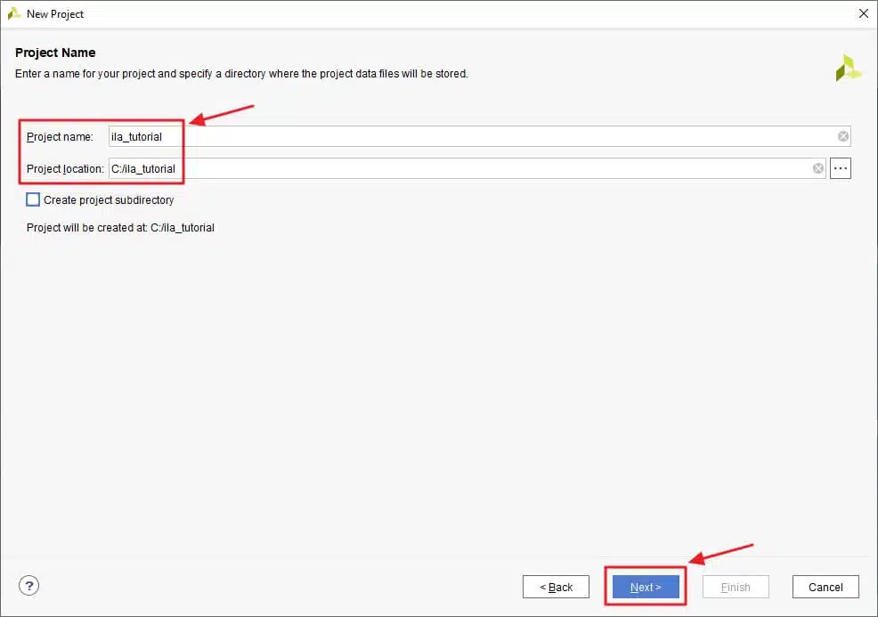
Change the name of the project to ila_tutorial and click on Next.
Note: Do not use spaces in the project name. Instead, use an underscore or dash.
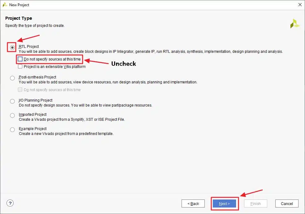
Choose RTL project and uncheck Do not specify sources at this time and click on Next to continue.
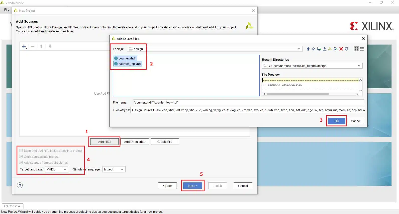
Add the source files; counter.vhdl and counter_top.vhdl from the design folder. Choose VHDL for the target language. Check Copy sources into project and click on Next to continue.
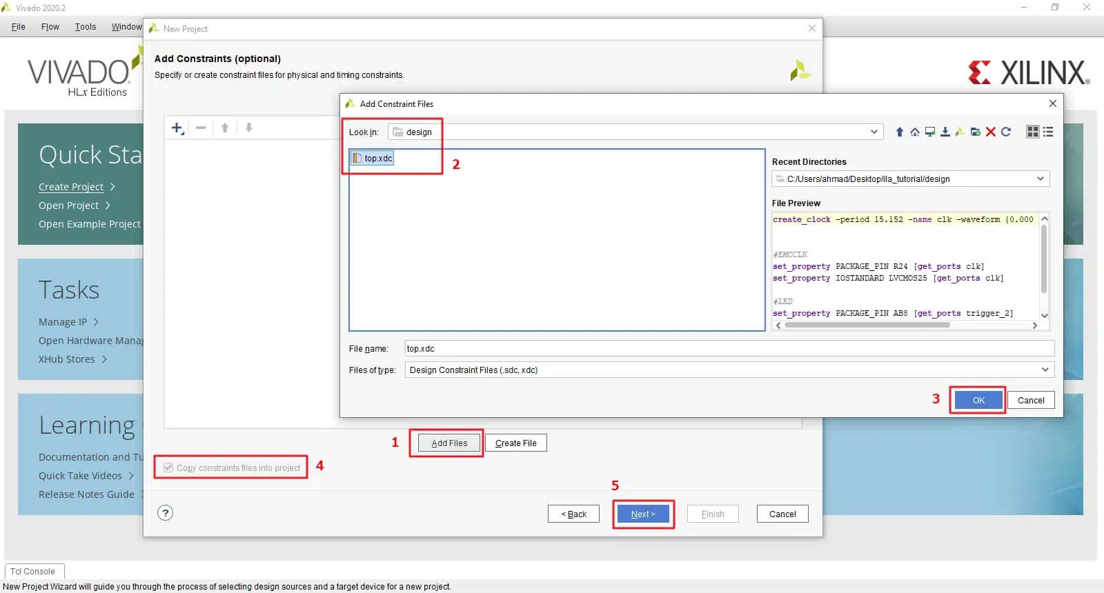
Add the constraint file top.xdc from the design folder. Check Copy constraints files into project and click on Next to continue.
Note: this constraint file is specific to the KC705 board. You need to change the clk pin and the led pin according to your board. And also, the -period of your board clock.
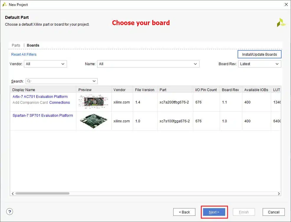
Search for your board and select it from the list. Click on Next to continue.
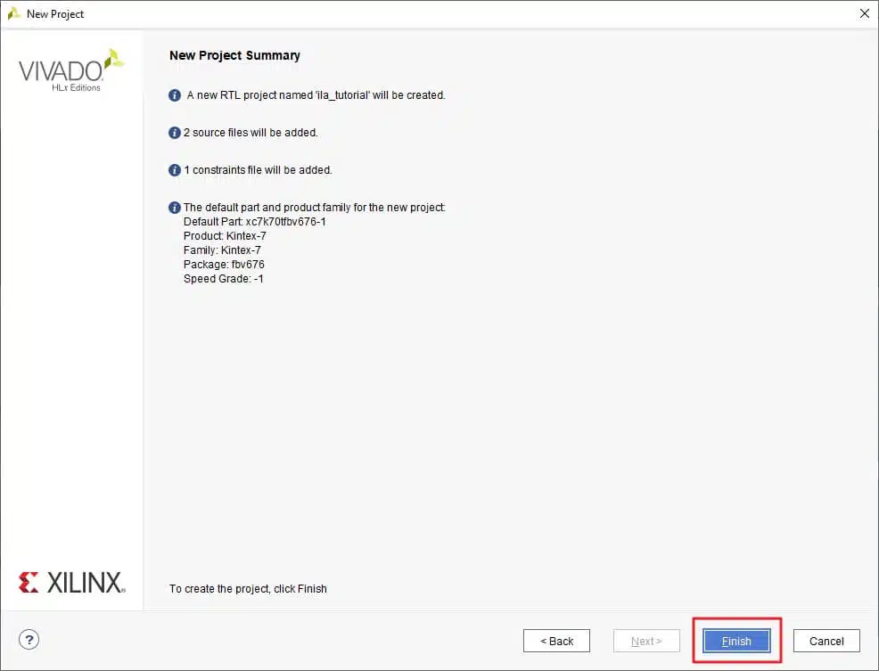
This is the final screen of the New Project wizard. Click Finish to open your project.
The design example explanation
We will use a simple two-counters chain example for this tutorial.
The counter.vhdl file contains the RTL code for a trivial 4-bit counter that counts from 0 to 15 when enabled. It asserts the 1-bit output when the count is between 12 and 15. For all other values, the output remains low ‘0’.
Here is the entity interface for the counter module.
----------------------------------------------------------------------------
-- ENTITY DECLARATION.
----------------------------------------------------------------------------
  ENTITY counter IS
    PORT(clk     : IN  STD_LOGIC;  -- Main clock
         reset   : IN  STD_LOGIC;  -- reset, active_high
         enable  : IN  STD_LOGIC;  -- enable the next counter
         trigger : OUT STD_LOGIC   -- trigger the next counter
        );
  END ENTITY;
The counter design has two internal signals: count and trigger_o.
– count is used to implement the counting functionality.
– and trigger_o is an intermediate signal for connecting the output port trigger.
Don’t worry about ATTRIBUTE, it will be explained later.
----------------------------------------------------------------------------
-- ARCHITECTURE DECLARATION.
----------------------------------------------------------------------------
  ARCHITECTURE rtl OF counter IS

    -- INTERNAL SIGNALS DECLARATION --
    SIGNAL count     : UNSIGNED(3 DOWNTO 0) := (OTHERS => '0');
    SIGNAL trigger_o : STD_LOGIC := '0';

    -- ATTRIBUTE DECLARATION --
    ATTRIBUTE MARK_DEBUG : STRING;
    ATTRIBUTE MARK_DEBUG OF count : SIGNAL IS "true";
In the listing below, we see the implementation for the counter. The seq_proc process is triggered on the rising edge of the input port clk and is in reset mode when the input port reset is high ‘1’.
The count signal is incremented when the input port enable is high ‘1’, and the trigger_o signal is asserted high when the value of the signal count is between 12 and 15.
seq_proc: PROCESS (reset, clk)
BEGIN -- for seq_proc
  IF (reset = '1') THEN
    count     <= (OTHERS => '0');
    trigger_o <= '0';
  ELSIF rising_edge(clk) THEN
    IF (enable = '1') THEN
      count <= count + 1;
      IF (count > x"B" AND count <= x"F") THEN
        trigger_o <= '1';
      ELSE
        trigger_o <= '0';
      END IF;
    END IF;
  END IF;
END PROCESS;
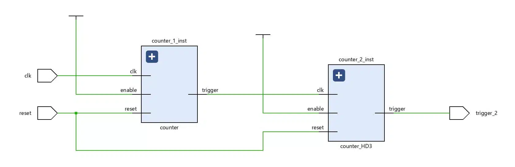
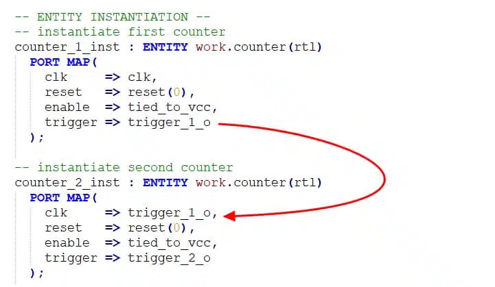
The file counter_top.vhdl contains two instants of the counter connected sequentially.
– The counter_1_inst is always enabled, and it clocks the counter_2_inst. That is, the output port trigger of counter_1_inst is connected to the input port clk of counter_2_inst.
– The resulted behavior is that counter_1_inst activates counter_2_inst only 4 out of 16 clock cycles. Thus, counter_2_inst will increment its counter four times each 16 counts.
Creating the VIO core for RESET
Now that you understand the design example, we will create a VIO to control the input port reset. That will give us the ability to manipulate (toggle) the reset from Vivado IDE so we can manually control when to start/stop the counters.
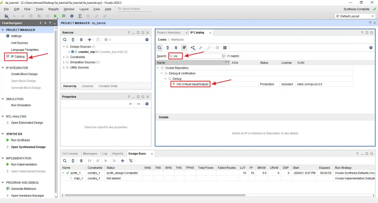
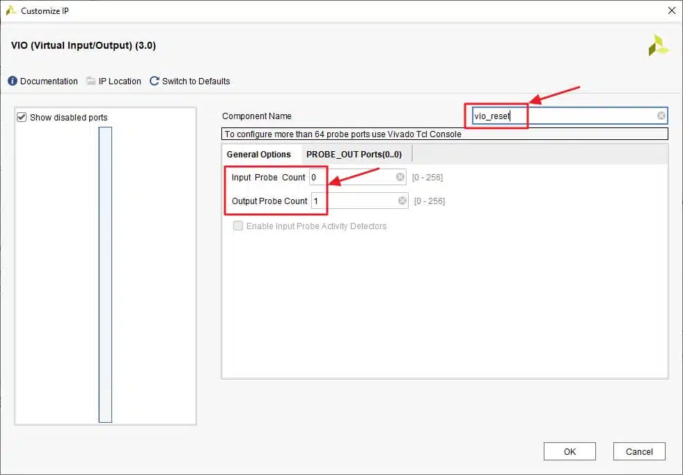
Click on IP Catalog, then search for VIO, then double-click on VIO (Virtual Input/Output).
First, we change the name to vio_reset.
Second, we only need an output port for the reset, so we put 0 in the input probe count box, and we put 1 in the output probe count box.
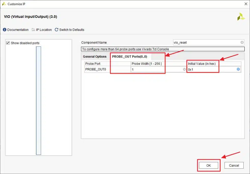
Click on the PROBE_OUT port tab. As reset is a 1-bit signal, we put 1 in the probe_width box, and we also put 0x1 in the initial value box so it starts with high ‘1’. Then click on OK and Generate. Vivado will now begin synthesizing the VIO.
After Vivado finishes synthesizing the VIO, we need to add it to our design by declaring a component for it and instantiating it in the counter_top.vhdl file as below.
First, add a component declaration for the vio_reset in the component declaration section in the counter_top.vhdl file.
-- Declare vio_reset
COMPONENT vio_reset
  PORT(
    clk        : IN STD_LOGIC;
    probe_out0 : OUT STD_LOGIC_VECTOR(0 DOWNTO 0)
  );
END COMPONENT;
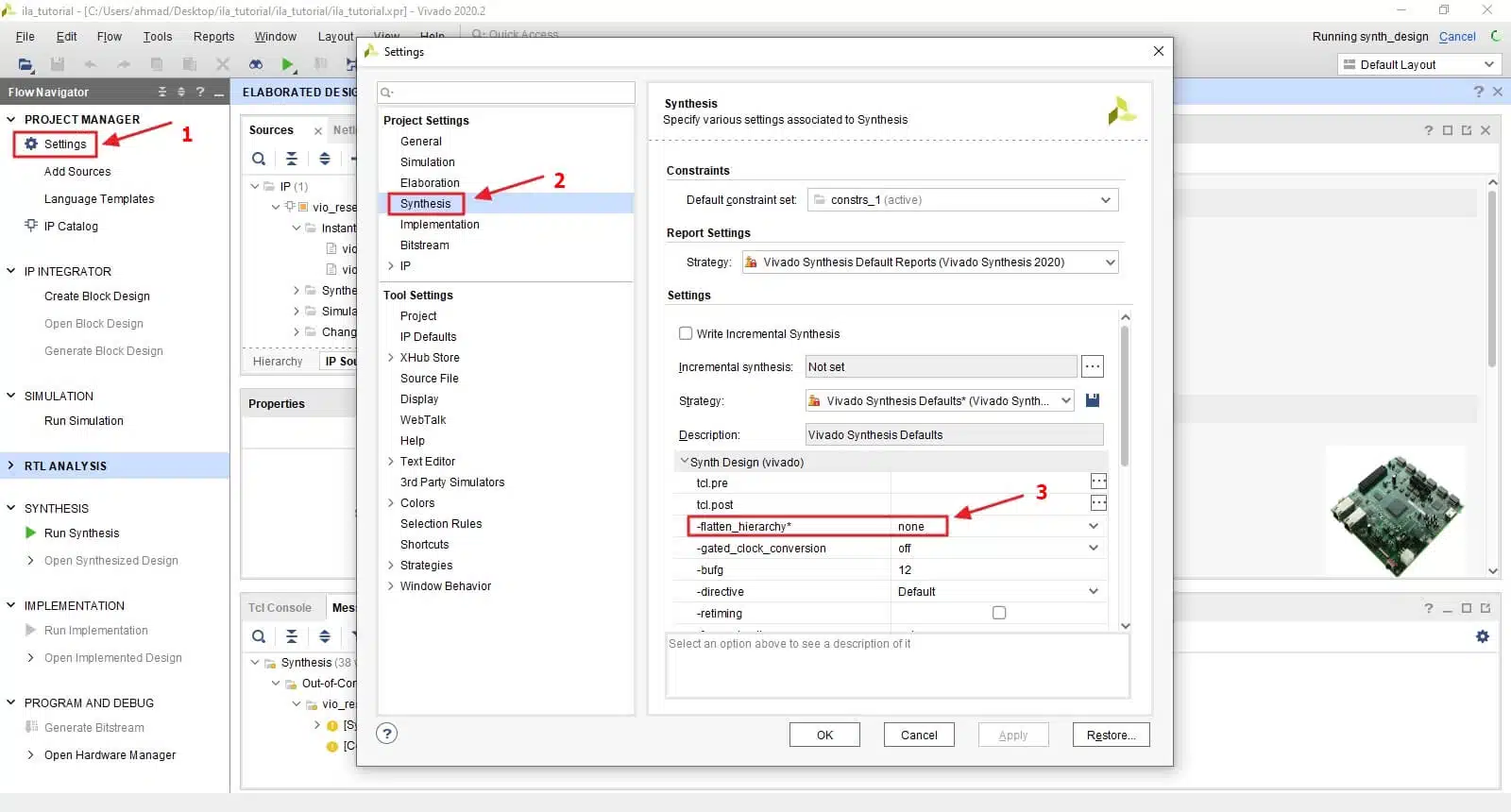
Now, the VIO is complete, and we are ready to synthesize the design. But before that, we need to change the synthesis setting flatten_hierarchy to None.
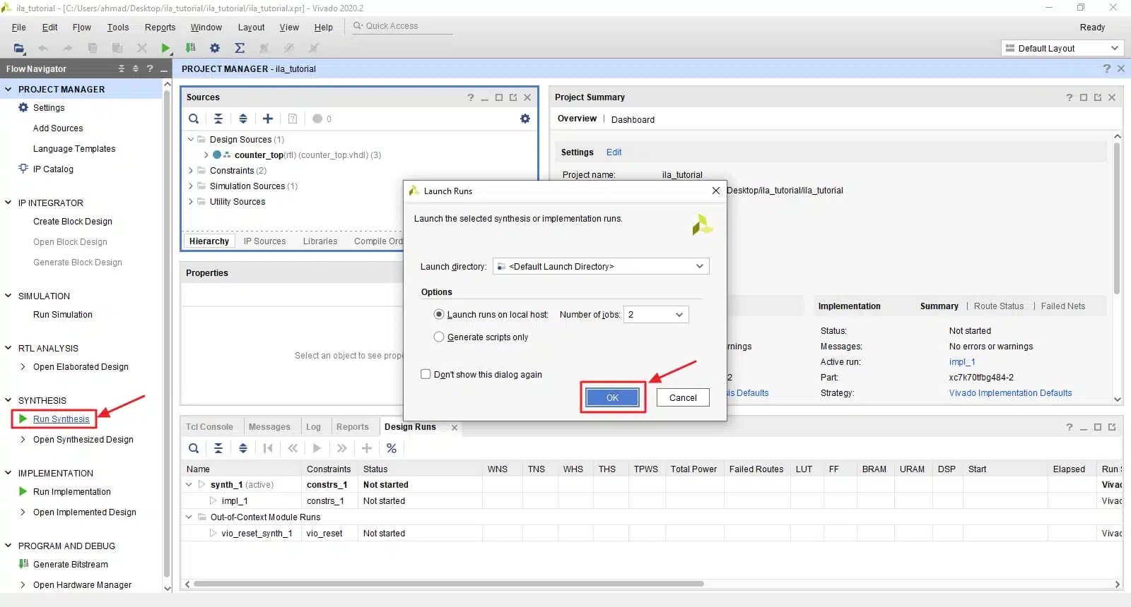
Click on Run Synthesis and then on OK.
When Vivado finishes synthesis, click on Open Synthesized Design.
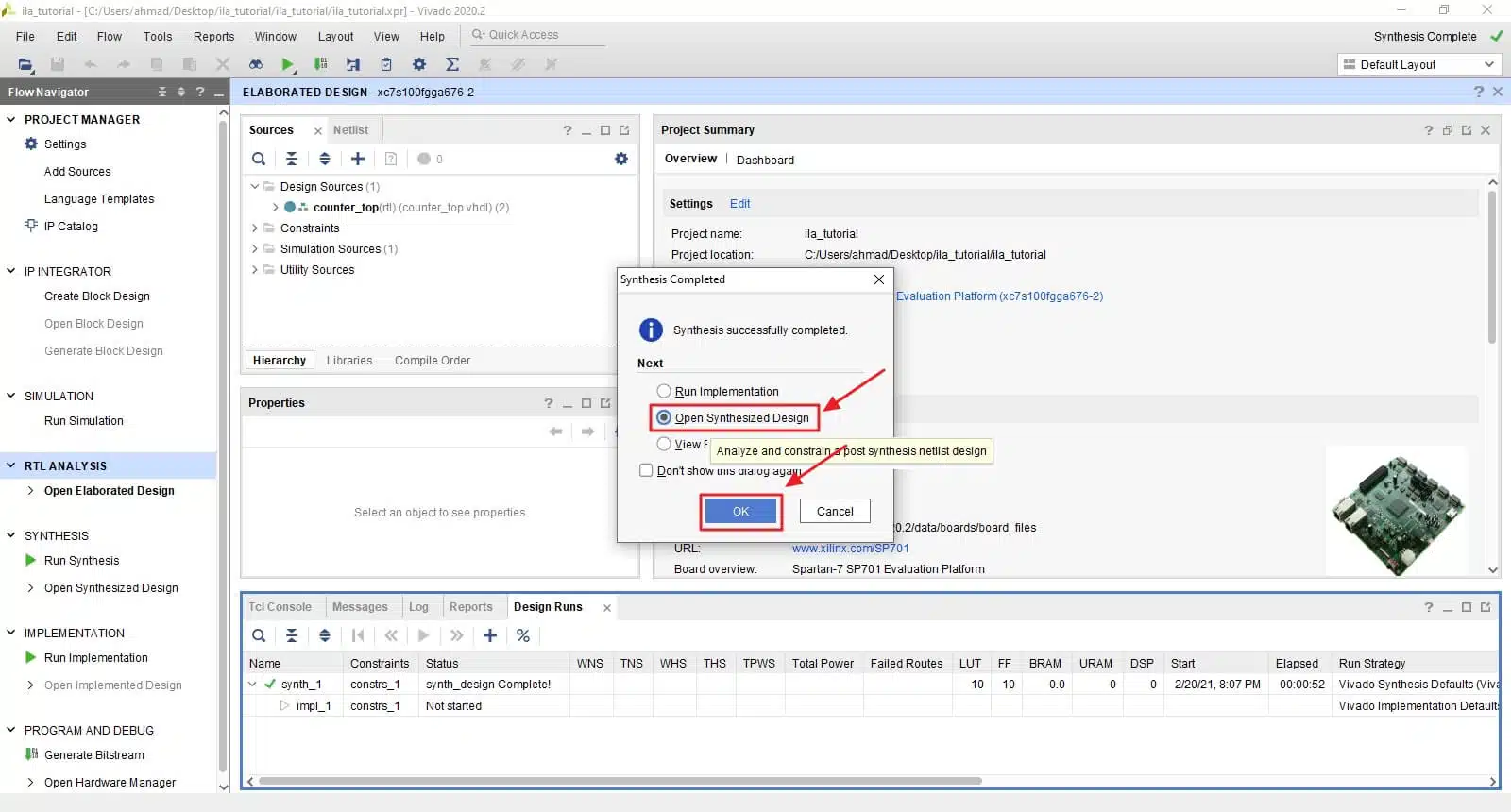
Change the layout to debug by clicking on Layout and then Debug.
Inserting debugging probe flow
Our synthesized design now contains the vio_reset instance, and it is time to specify the signals that we want to probe. There are three ways to do that:
- Insertion from VHDL file
- Insertion from the Netlist
- Insertion from xdc/tcl file
We will use the first two methods and leave the third for a later tutorial.
Insertion from VHDL file
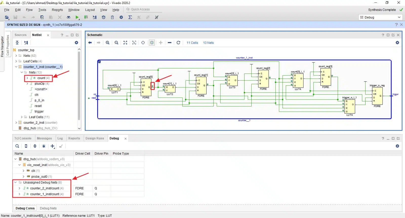
This method is the easiest and fastest way to insert a probe, especially when it’s a composite type (array or record). But it requires adding code to the design files, VHDL code that’s redundant in the real product.
We can insert a probe in the VHDL design file by:
- Declaring a special attribute called MARK_DEBUG
- Attach the signal that we want to probe with this attribute
- And activate it by giving it the value “true” as below:
-- ATTRIBUTE DECLARATION --
ATTRIBUTE MARK_DEBUG : STRING;
ATTRIBUTE MARK_DEBUG OF count : SIGNAL IS "true";
Note: we only need to declare the attribute once in each VHDL design file, allowing us to attach it to multiple signals.
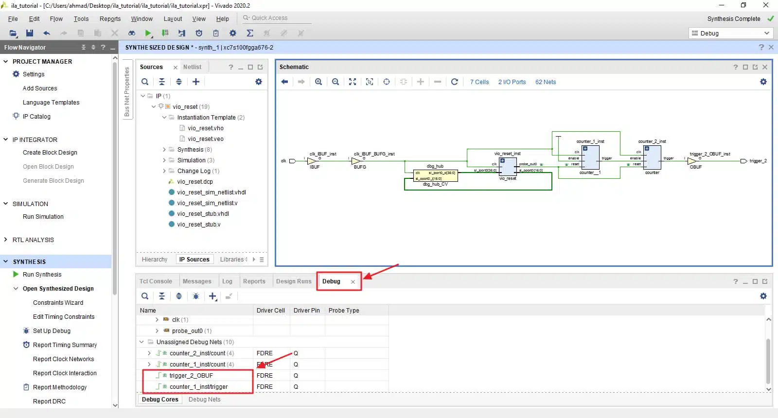
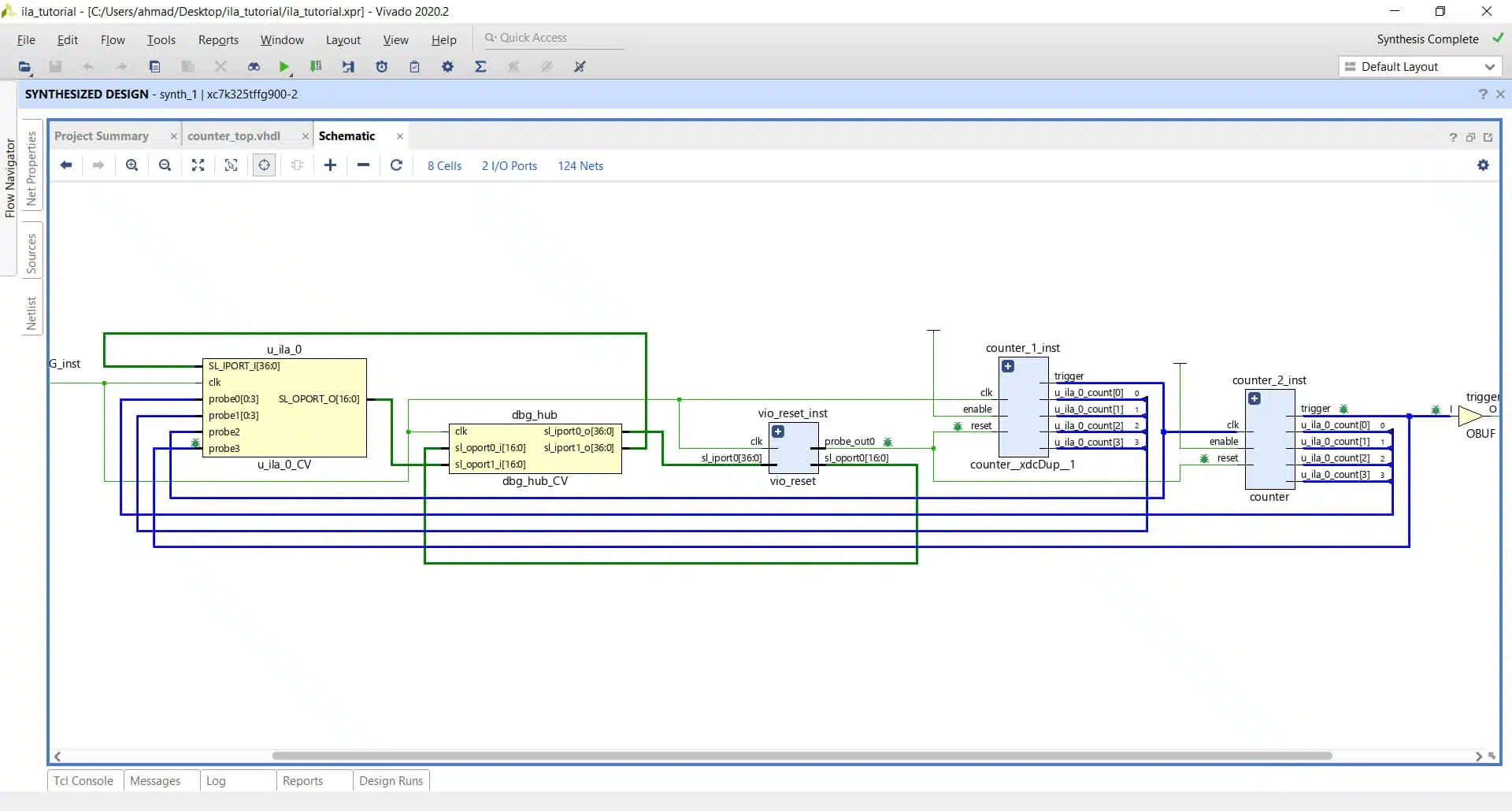
We can see from the synthesized design that the signal count in both counter_1_inst and counter_2_inst are listed under Unassigned Debug Nets and marked with a bug icon in both the Netlist and the Schematic.
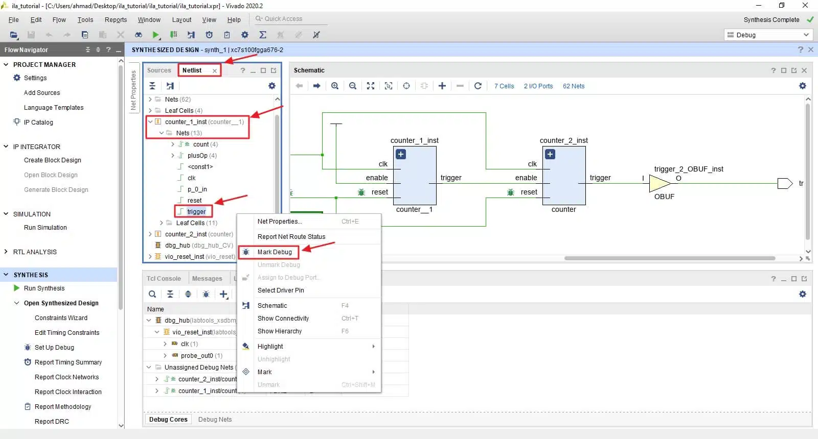
Insertion from the Netlist
This insertion method is also easy, but it requires that you first synthesize the design and then manually click on each signal to mark it for debugging. It could be exhausting if the design is large and you want to monitor many signals.
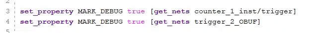
We will probe the output port trigger in both counters using the Netlist. We can do this either from the Netlist window or the Schematic by locating the signal net and then right-click on it and choose Mark Debug.
From the Netlist window, find trigger under counter_1_inst → Nets → trigger. Then, right-click on it and choose Mark Debug.
From the Schematic window, find trigger output from counter_2_inst. Then, right-click on it and choose Mark Debug.
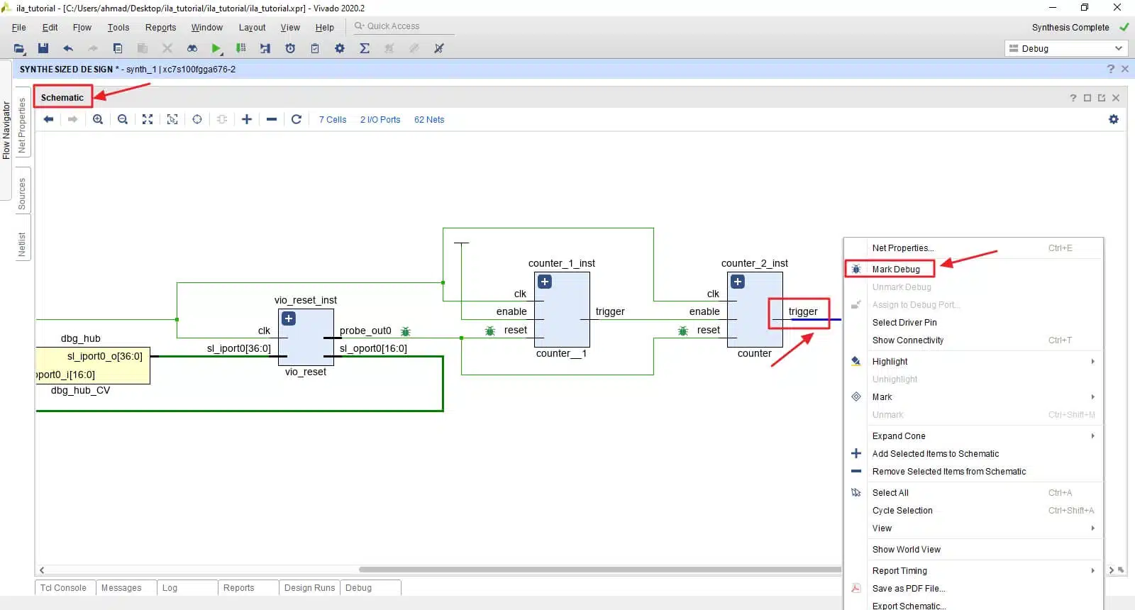
We can see that they now are listed under Unassigned Debug Nets.
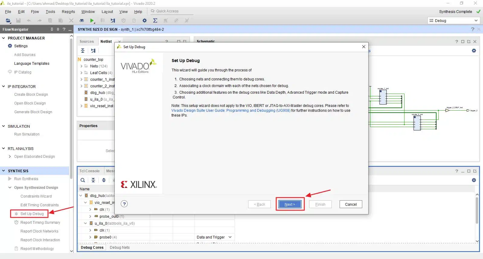
Creating the ILA debug core
Now it is time to create the ILA debug core. We need to create a probe for each signal that we want to analyze. The easiest way is to take advantage of Vivado wizard Set Up Debug.
Click on Set Up Debug and then click on Next.
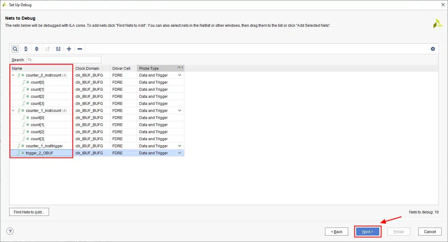
Vivado will list all the debug signals and capture the clock domain for you automatically. Here we see that our four signals are listed. You can remove the signals that you are not interested in or add extra signals, but we will use all of them.
Note: we don’t have to use all the signals that we have marked as Debug.
Click on Next.
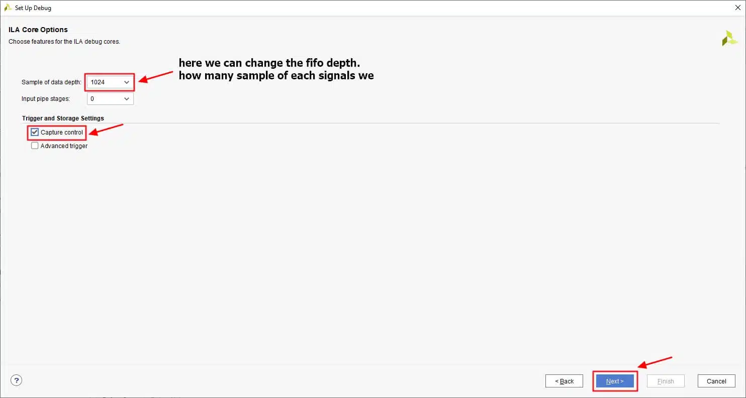
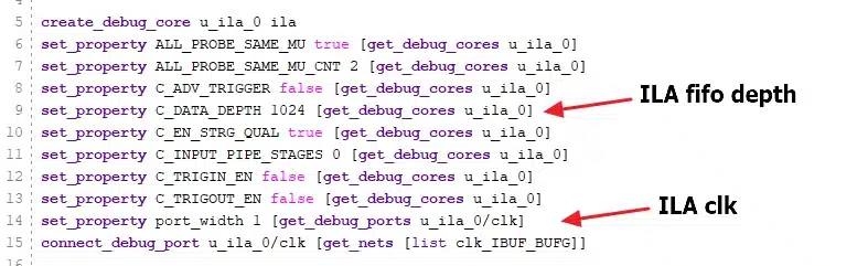
Now we configure the ILA by choosing the FIFO depth and checking Capture control. We can leave the FIFO at 1024 as it is enough depth for our example.
Click on Next.
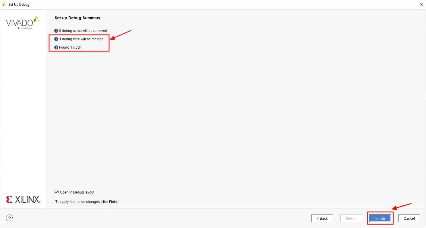
Now we see that Vivado found one clock and will create one debug core.
Click on Finish.
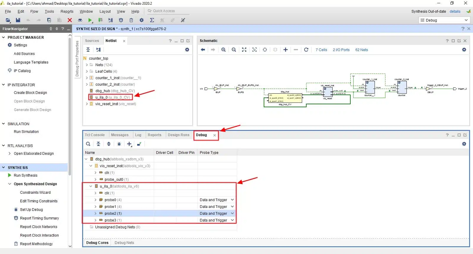
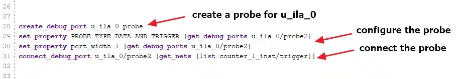
We can now see an ILA debug core with four probes added to the debug tab and the Netlist window.
IMPORTANT: It is very important to save the constraint in this stage so it can be added to the design. Otherwise, we risk losing our ILA core.
Click the Save icon or hit Ctrl+S.
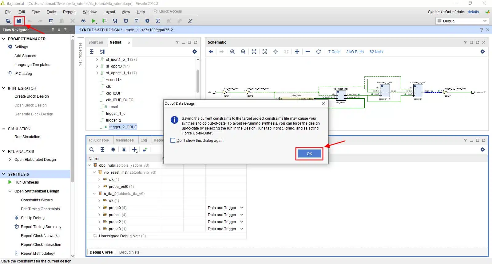
Name the file ila_core and click OK.
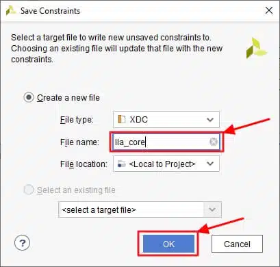
The ila_core.xdc file will be added to the constraint, and it includes the code and settings for the ILA.
Let us take a look at the file content. You can open the file by going to the Source window → expand the constraint folder → expand constr_1.
First, we see that the file adds a debug attribute to the signals that we marked debug using the Netlist insertion.
Next, we see the creation and configuration of an ILA core.
Next, we see the creation, configuration, and connection for each probe.
Next, we see the creation of a debug hub (dbg_hub).
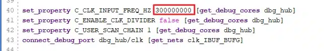
The debug hub is responsible for the communication between Vivado IDE and the debug cores (ILA and VIO). We see that it defines a clock frequency (default is 300 MHz). You need to change that clock to match your clock frequency and save the file.
Note: the clock connected to ILA and Debug_hub must be a free-running clock.
Now, the ILA is completed and saved. We need to rerun the synthesis so the ILA can be added to the synthesized design.
Click Run Synthesis and then on OK.
When Vivado finishes running the synthesis, click on Open Synthesized Design and then on Schematic.
We can see now that Vivado has added the ILA and Debug_Hub to our design and has connected the debug signals to the ILA probes.
Now we are ready to implement our design and generate the bitstream so we can test our design.
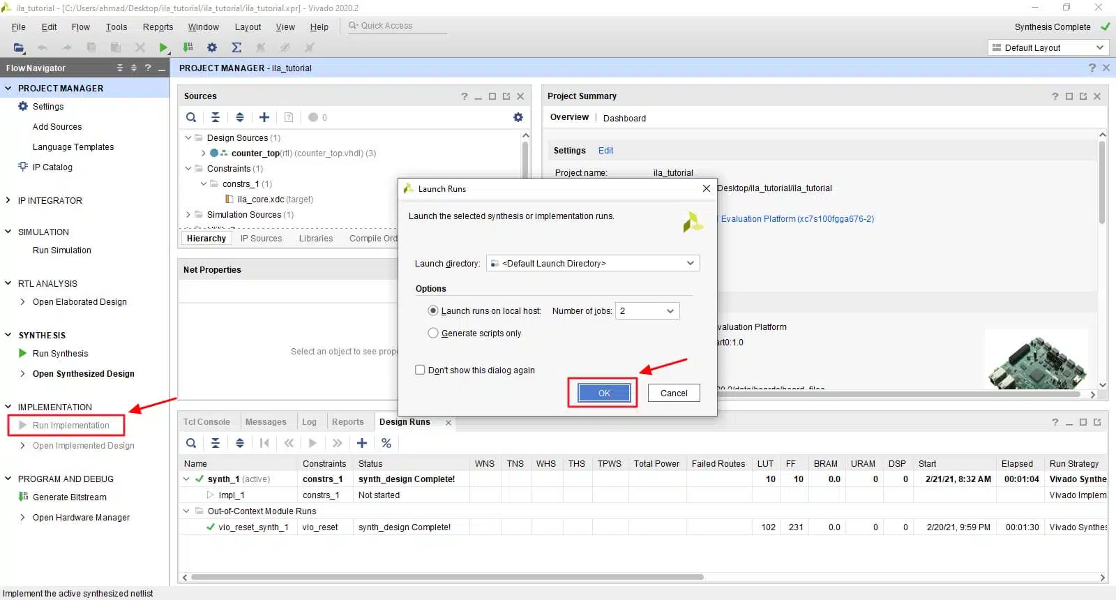
Click on Run Implementation and then on OK.
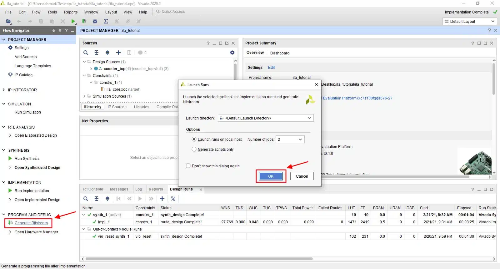
After Vivado finish running the implementation, click on Generate Bitstream and then on OK.
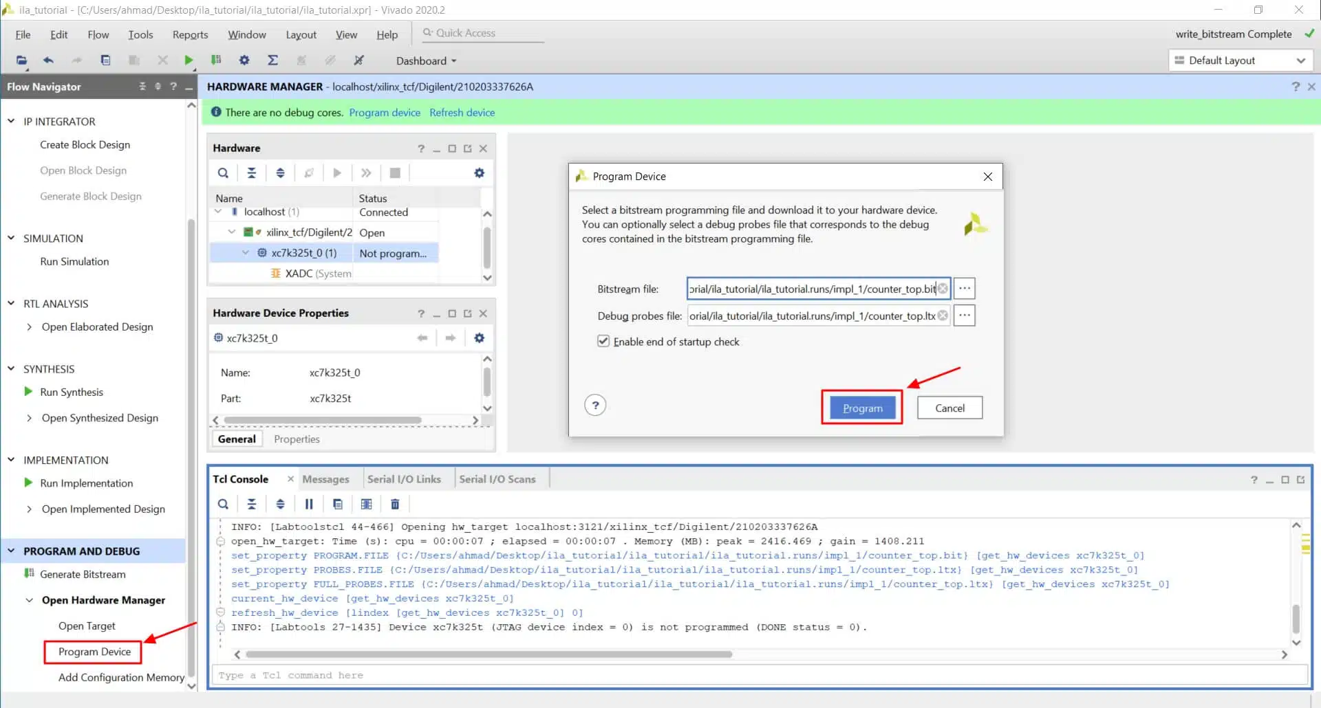
After Vivado finishes generating the bitstream, click on Open Hardware Manager and then on Open Target, and finally on Auto connect.
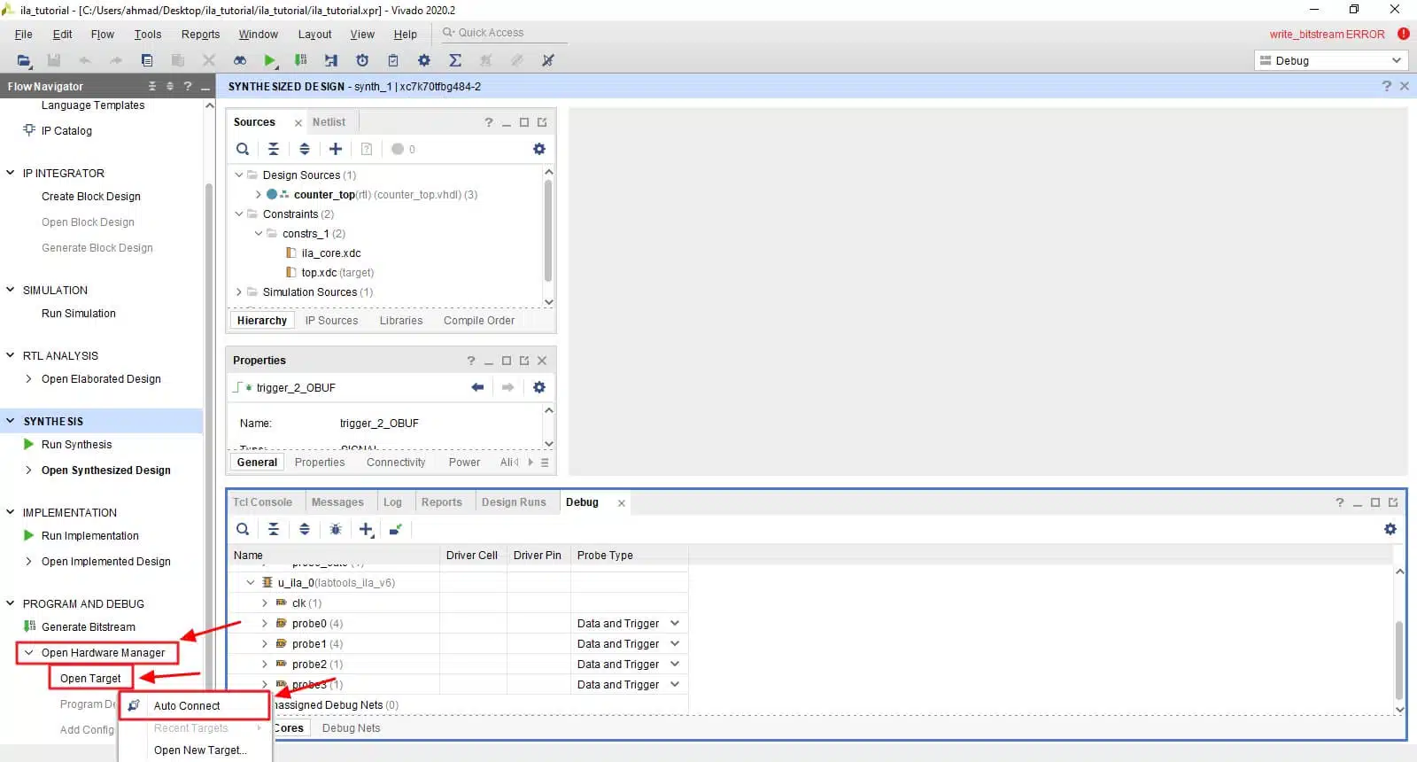
Next, we need to program the FPGA with the bit file (*.bit) and the debug probe file (*.ltx). Vivado automatically finds them for you.
Click on Program Device and then on Program.
Configuring the ILA triggers
After programming the device, we can see that Vivado’s GUI layout has changed, and a new hw_ila_1 dashboard has opened, containing several windows.
We will minimize some windows that we don’t need so we can work comfortably.
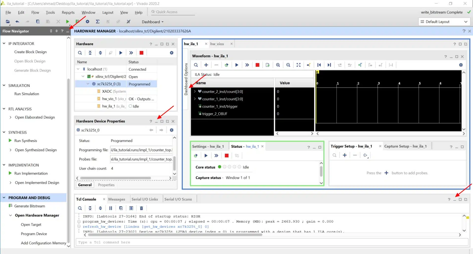
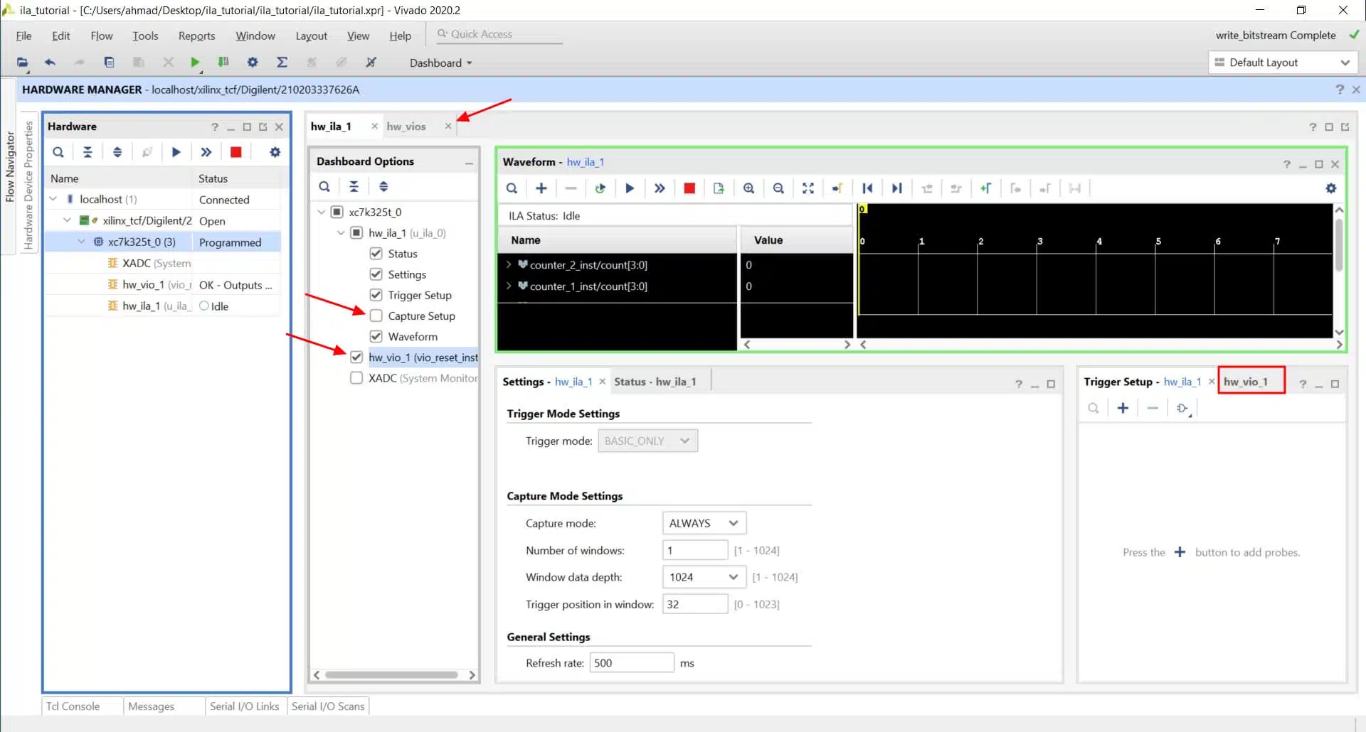
From the dashboard options, check hw_vio_1 and uncheck Capture Setup.
Also, close the hw_vios tab because when we checked hw_vio_1, it has been added to the Trigger setup window.
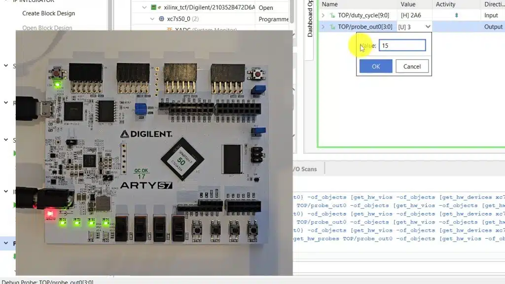
Now, we need to add the reset button to the VIO so we can control the reset.
Click on hw_vio_1 and then add reset as shown in the picture below.
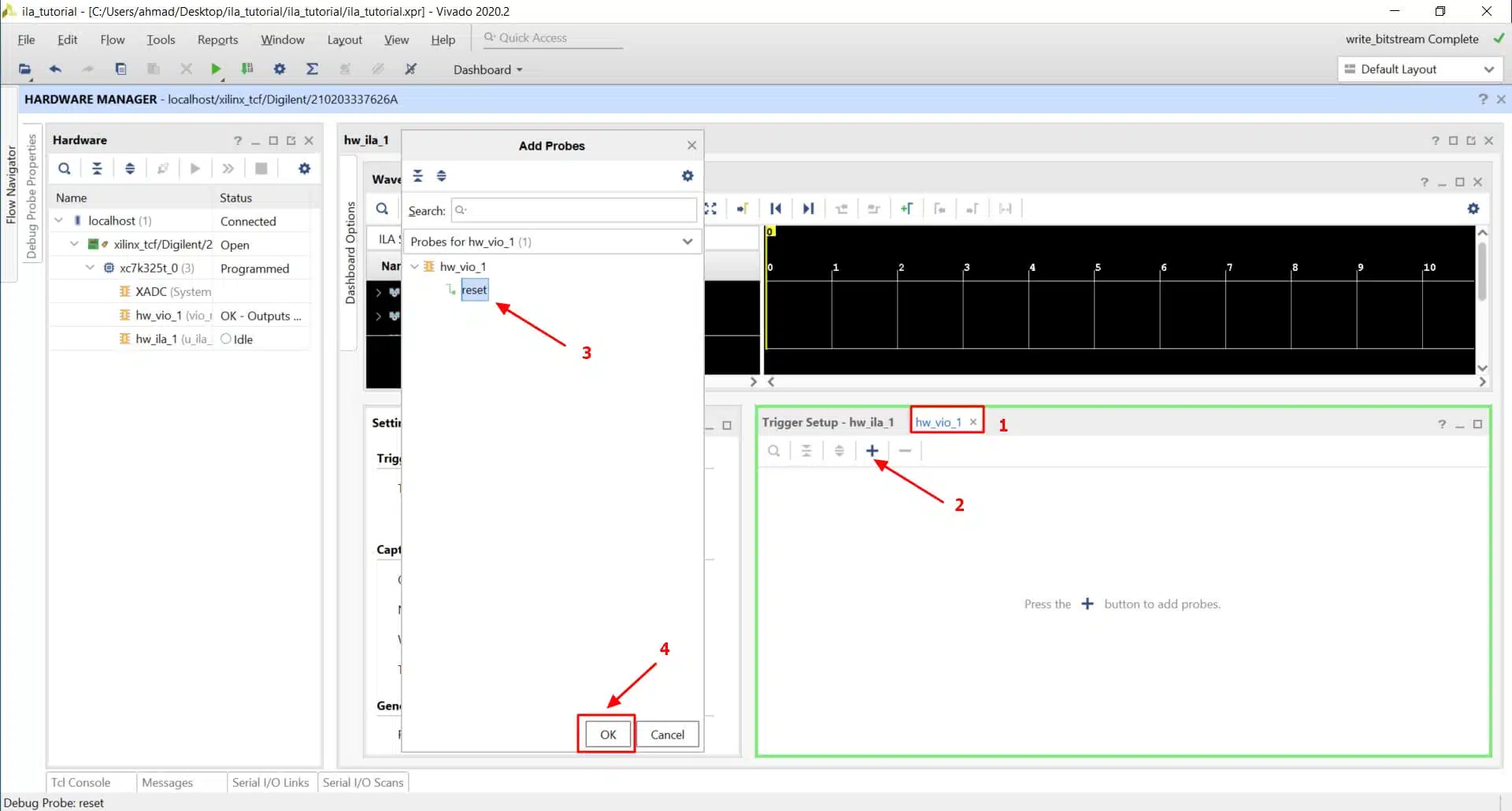
We can see that hw_vio_1 now contains the reset probe.
Change the value of the reset in vio_reset to 1 if it’s not 1.
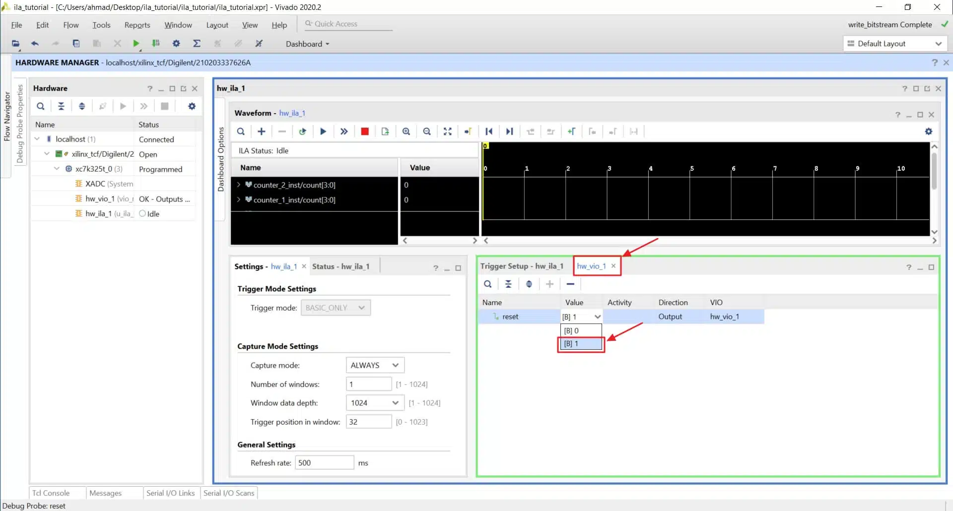
Now, we will add the triggers that we will use. A change of value on a trigger signal will cause the ILA to start recording the probed signals.
Let us say that we want to trigger (start recording) on the rising edge of the output port trigger of counter_1_inst. To do that, follow these steps:
- Go to the Trigger Setup – hw_ila_1 window
- Click on the + icon to add a new trigger and choose counter_1_inst/trigger and click on OK.
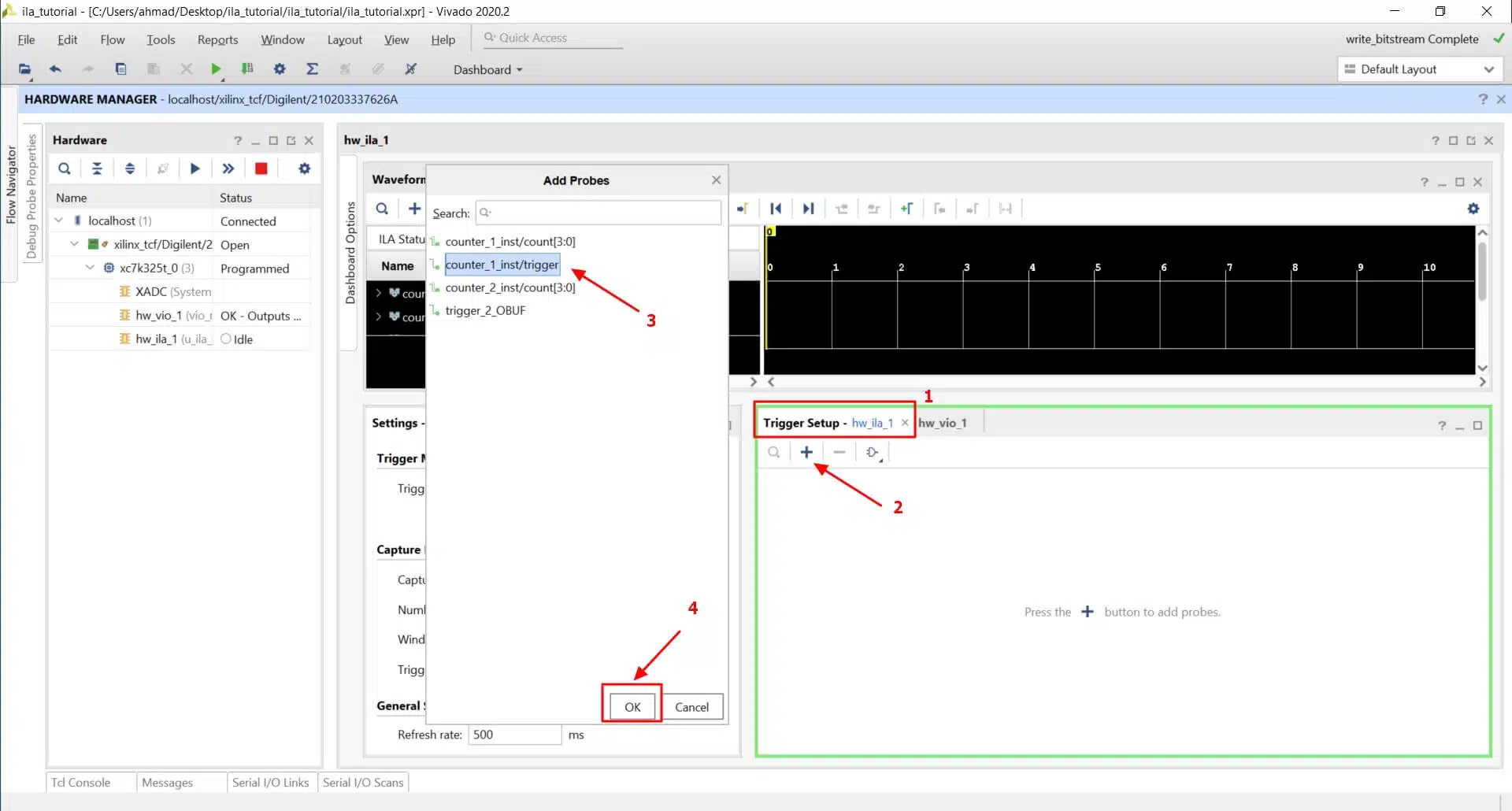
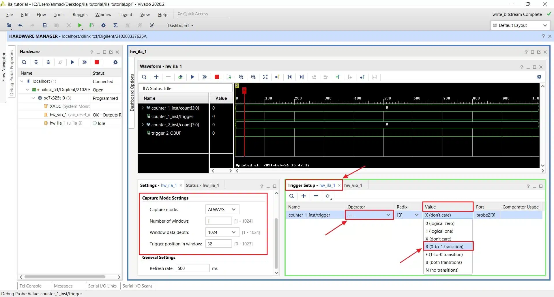
- We can see that the trigger has been added, and now we need to set up the condition. Click on the Value box and choose R(0 to 1 transition). Click on the Operator box and choose == (equal)
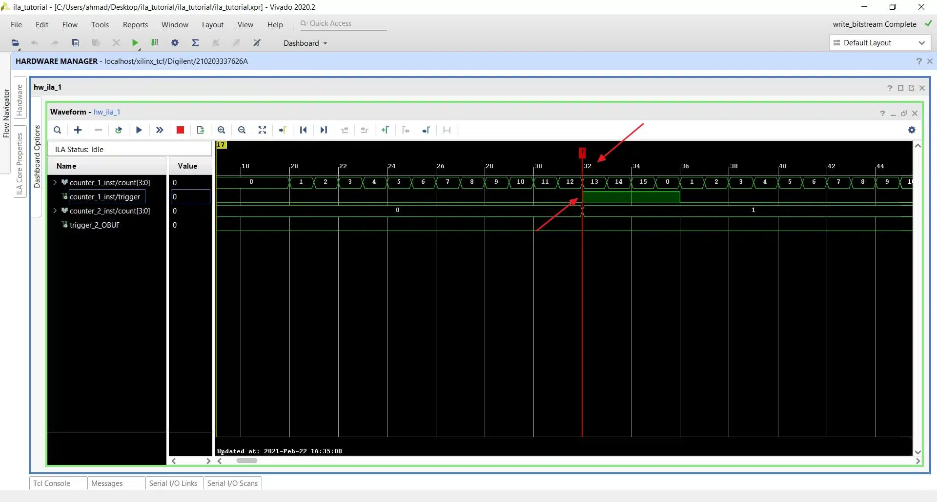
We will also change the trigger position to 32, meaning that it will record 32 samples before the trigger event in addition to what comes after.
Now, the trigger is set up and ready to be armed.
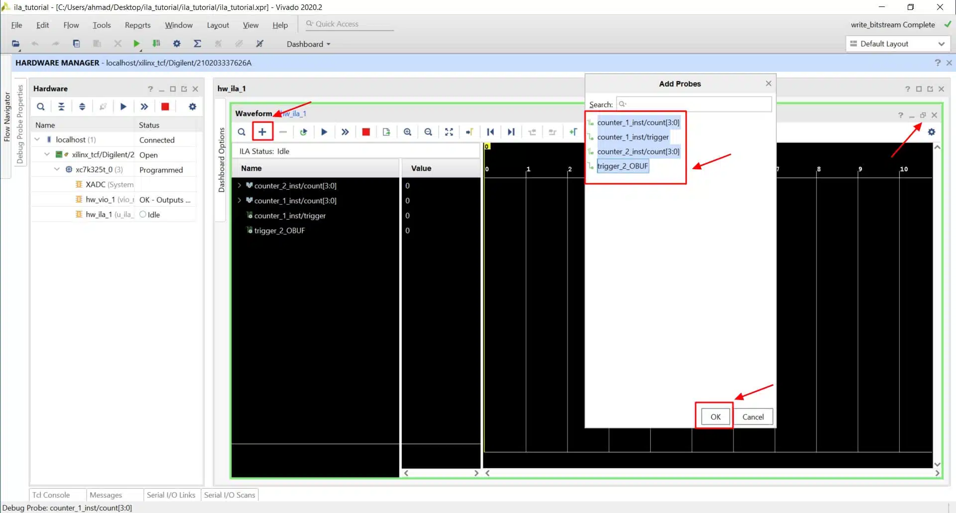
Now, we move to the waveform window to add the signals that we want to view. First, let’s maximize the inner window to gain a better view.
Second, we need to add some missing signals to the probe. Vivado usually adds all the assigned signals automatically, but in this case, it didn’t.
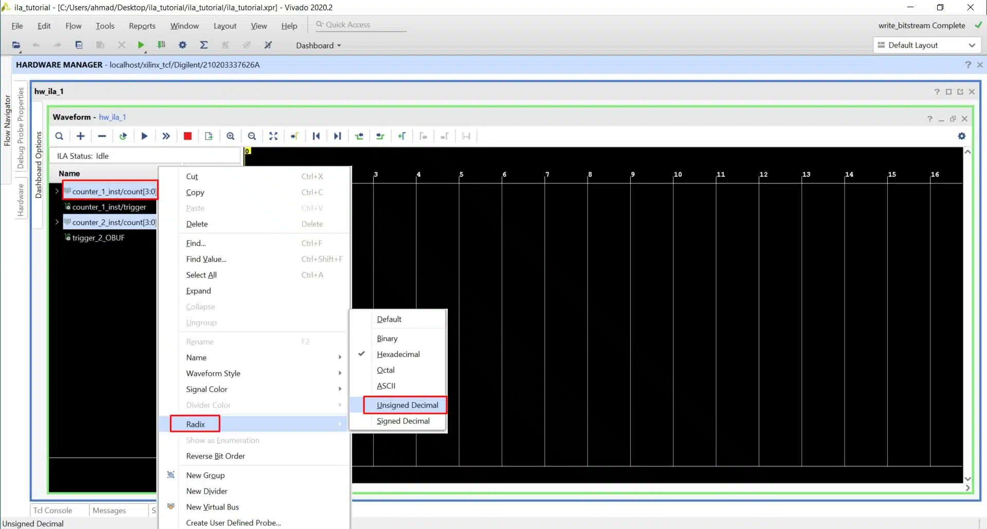
Now, we change the radix of the count signal to Unsigned as it is easier to follow.
Right-click on the count signal name and then choose radix and then Unsigned.
Running the ILA and VIO
Now, we have finished configuring and customizing the ILA, and we are ready to run it.
ILA has two running modes: Immediate and trigger.
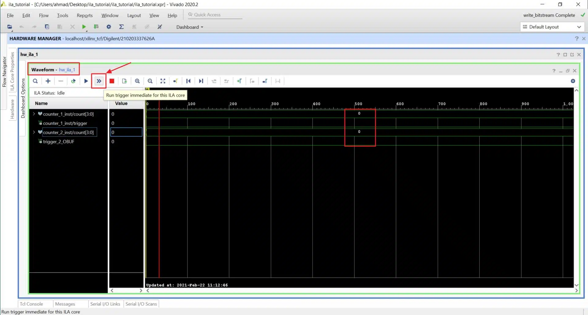
Immediate mode
Immediate mode triggers the ILA immediately and starts recording the samples directly until the FIFO is full.
Click on the Run trigger immediate button.
We can now see the recorded samples in the waveform window. We see that both count signals are 0, and both trigger signals are low ‘0’ because the reset is active.
Trigger mode
Trigger mode requires that we set up a condition for at least one trigger and arm it. The ILA will keep waiting for the armed trigger’s condition to become true, and then it will start recording the samples directly until the FIFO is full.
We have already added the trigger and set it up to R(0 to 1 transition).
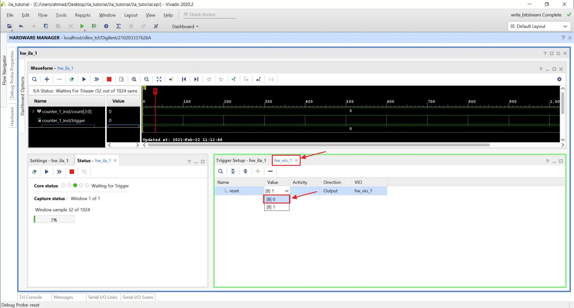
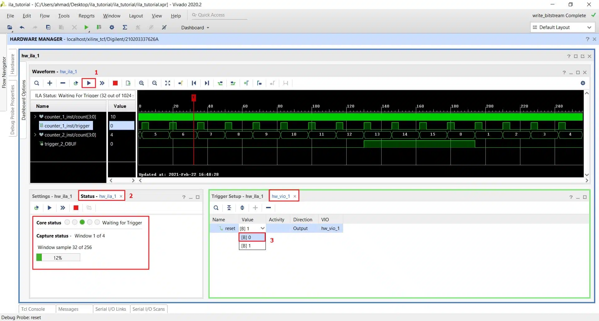
Running ILA with one trigger
Change reset back to 1 from vio_reset.
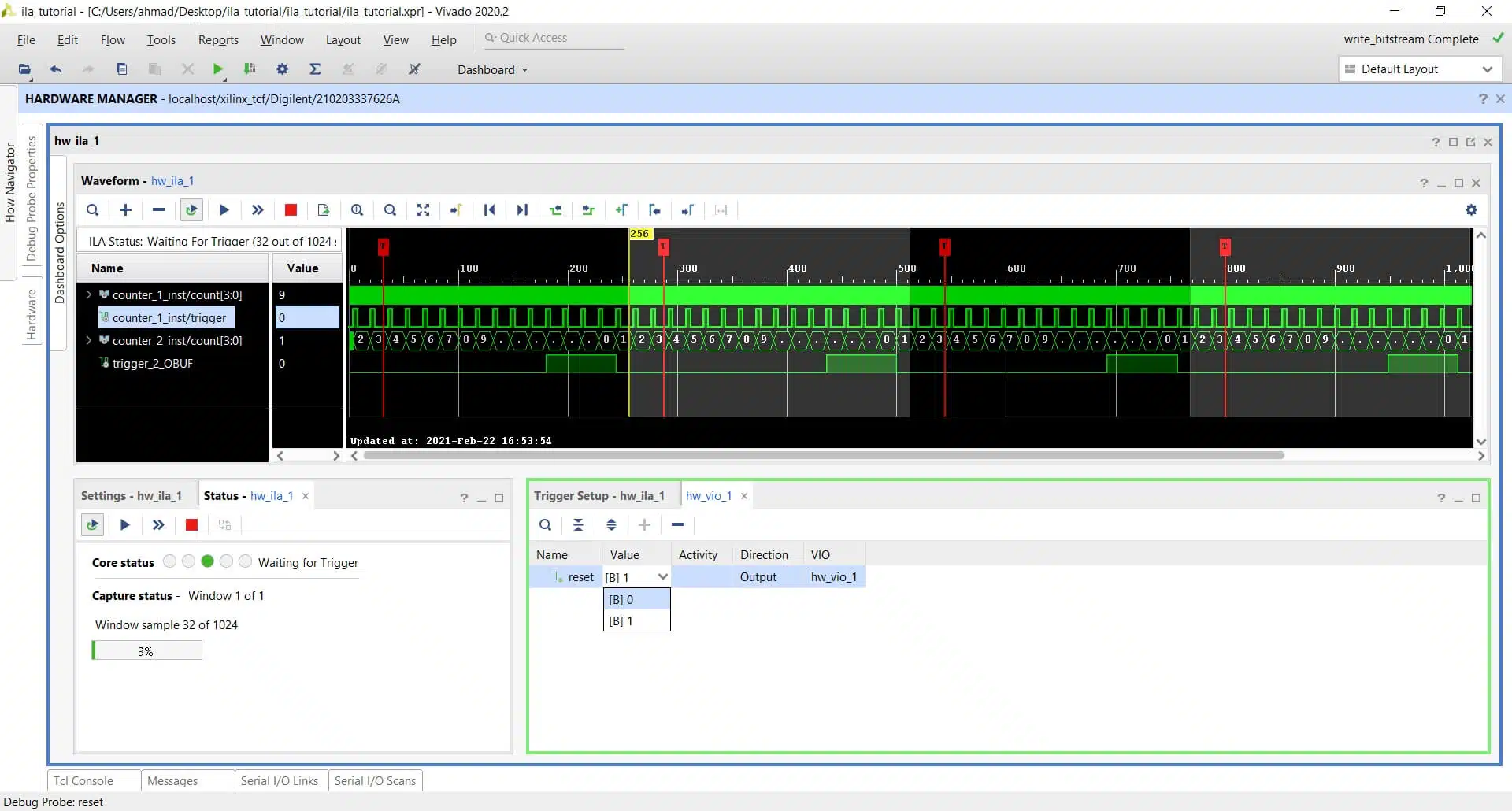
Click on the window Status hw_ila_1. We see that the core status is Idle as there are no triggers armed. Click on the Run trigger button, and that will arm the trigger.
We see now that the core status changed to waiting for trigger. As the reset is high, there is no activity on our trigger signal (port trigger of counter_1_inst), and ILA is waiting.
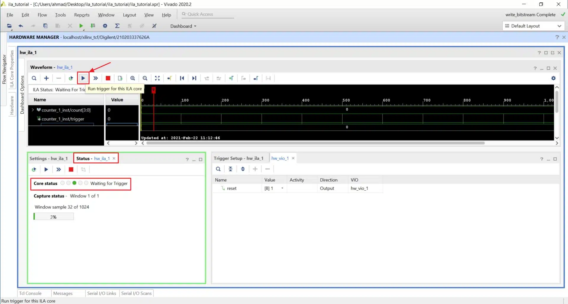
Now, let us change the reset to 0 so that the counters start working.
We see now the ILA has got triggered and has recorded the samples, and the core status changed back to Idle.
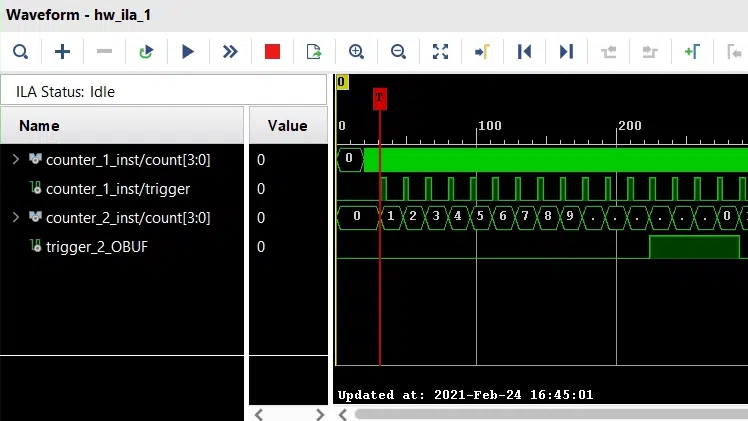
We see the red vertical line (marker) on the rising edge of our trigger signal (port trigger of counter_1_inst), and it is in position 32. We also can verify that the signal count is behaving correctly and the signal counter_1_inst/trigger is high for four clock cycles between 12 and 15 (the output is delayed by one clock cycle).
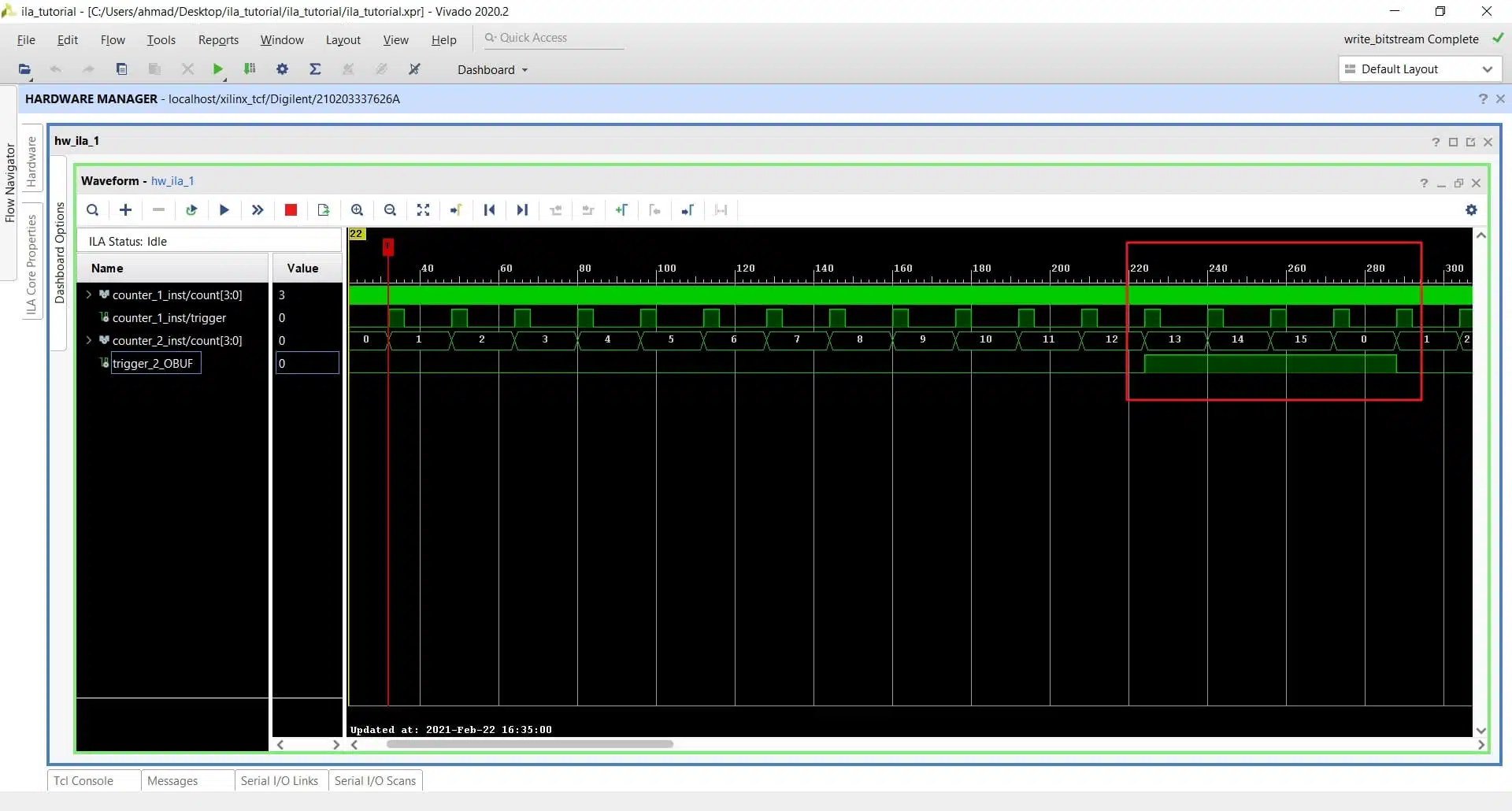
If we zoom out a little bit, we can also verify the behavior of count and trigger signals for counter_2_inst.
Running ILA with multiple triggers
We can use a combination of triggers for complex or advanced conditions. To capture several disjoint time frames in the same waveform, we can use multiple triggers that fire repeatedly.
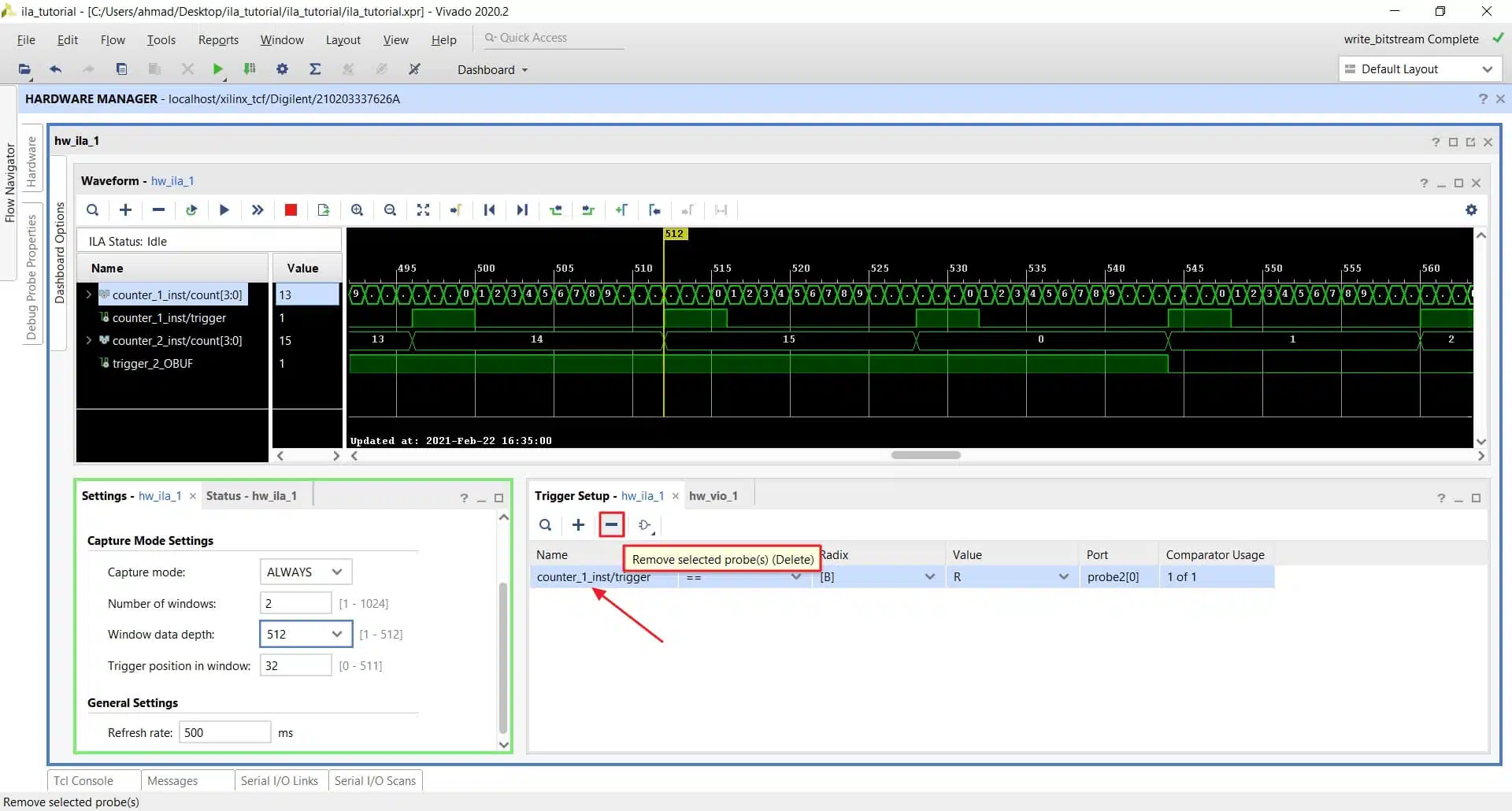
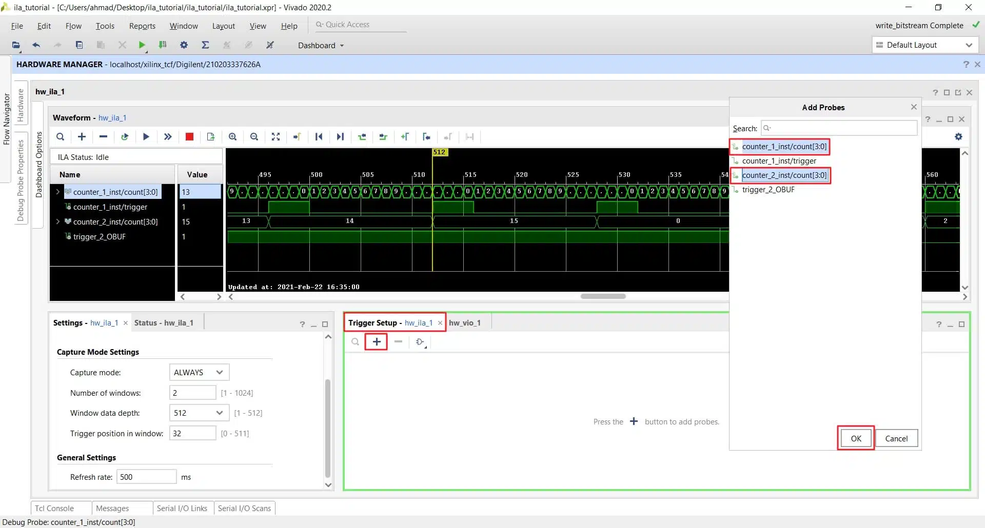
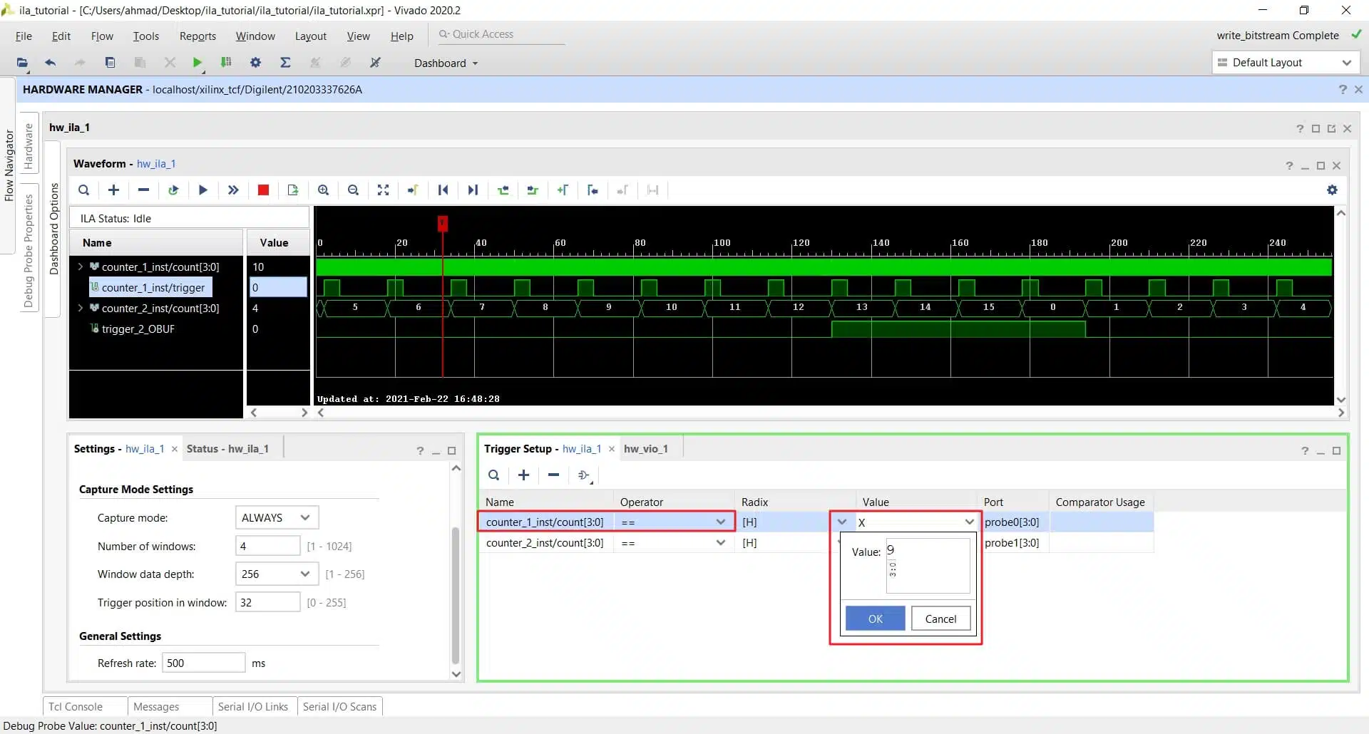
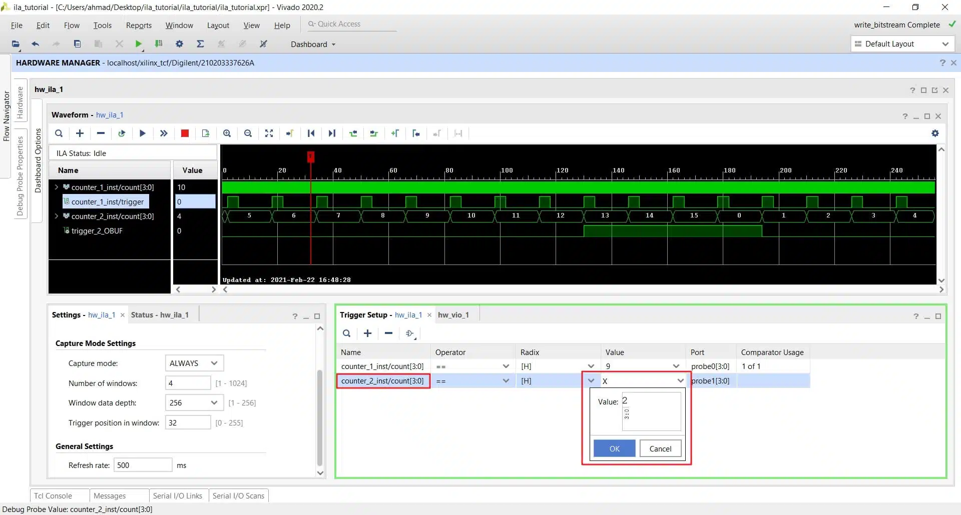
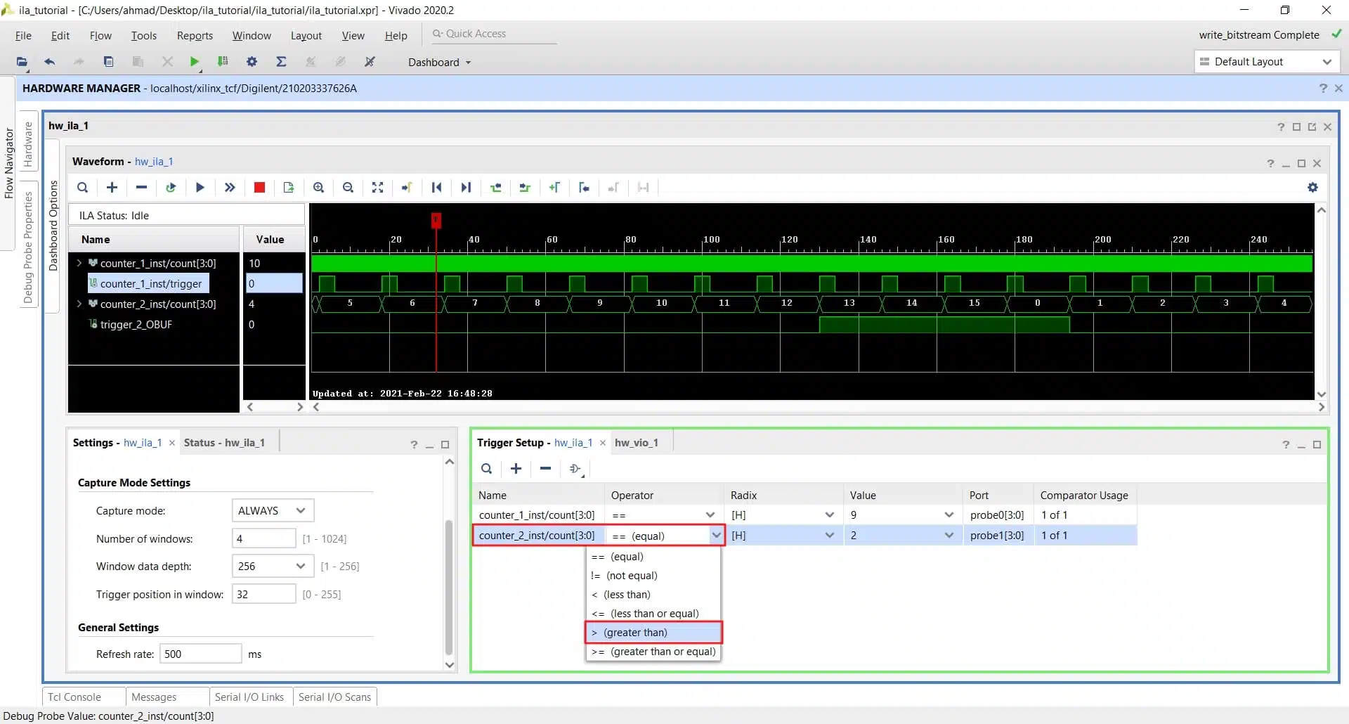
For example, let’s say we want to trigger when the count signal from counter_1_inst is equal to 9 (count == 9) and when the count signal from counter_2_inst is greater than 2 (count > 2). To do that and split the FIFO into four time windows, follow these steps:
- Change reset back to 1 from vio_reset
- Remove the previous trigger probe:
- Add both count signals as triggers:
- Configure the signal count for counter_1_inst to (count == 9):
- Configure the signal count for counter_2_inst to (count > 2):
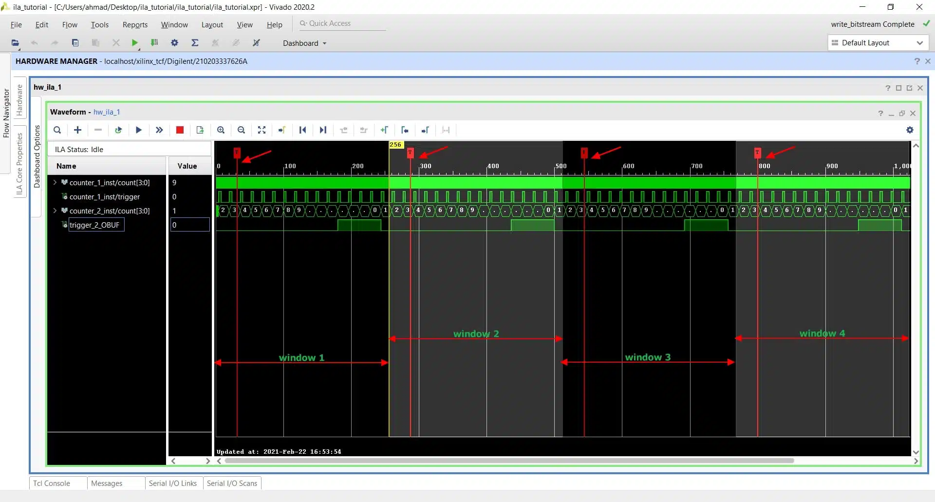
- Configure the number of windows to 4 and FIFO depth to 256, and position to 32.
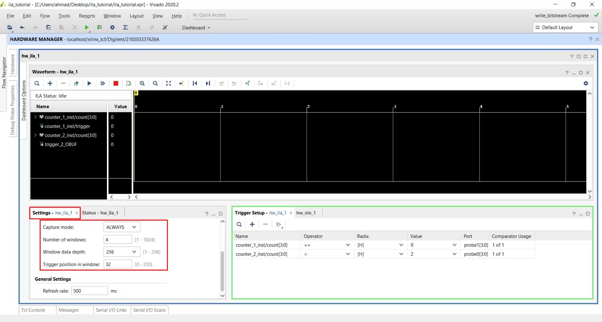
- Click on the Run trigger button, and that will arm the trigger. Notice that in the window Status hw_ila_1, the capture status is now window 1 of 4 because we have four windows.
Change reset back to 0 from vio_reset.
Maximize the waveform window. We see now that we have four windows and a trigger associated with each window. Notice that these windows are independent and not continuous.
The ILA waits for the trigger event to happen, and when it does, the ILA uses the first window to record 256 samples. It then immediately waits for the next trigger until all the windows are full.
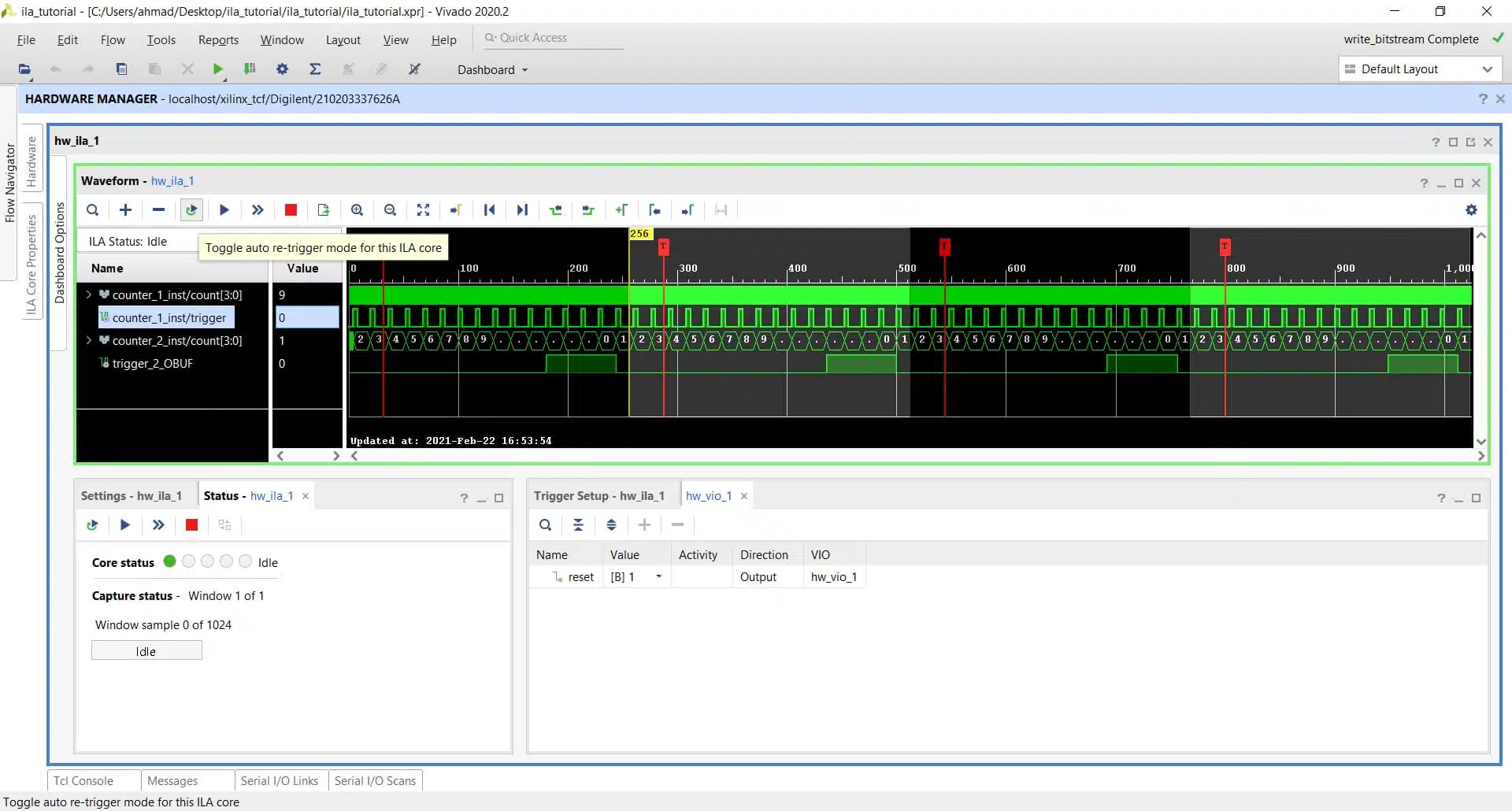
Running ILA with Auto re-trigger mode
ILA has a nice feature called Auto re-trigger that will automatically arm the trigger after it gets triggered. It is useful when monitoring events that occur seldom and you want to run a test overnight. Or you can use it when the trigger happens so often and fast that you cannot arm the trigger manually to capture the samples repeatedly.
Let us assume that the output port trigger of counter_2_inst gets asserted every 3 hours, and you want to record the data each time it happens. To use the Auto trigger, follow these steps:
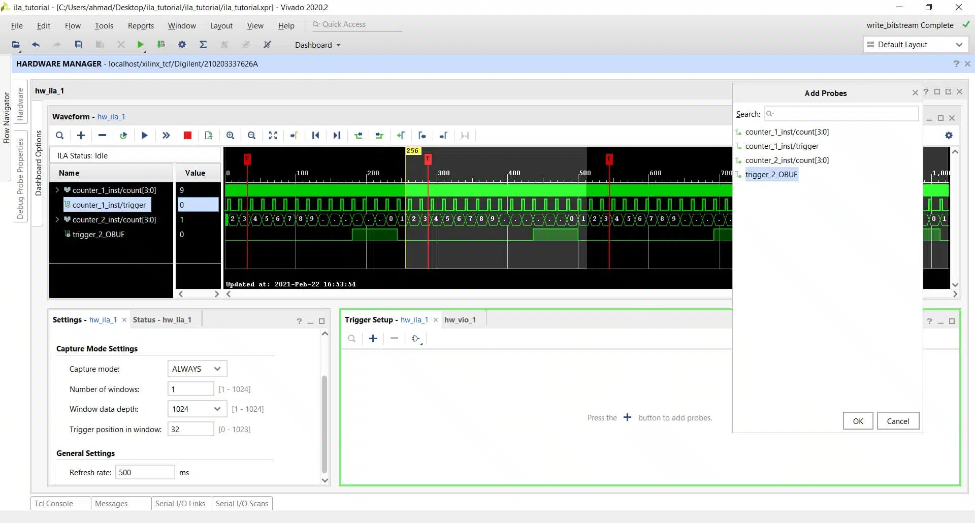
- Change reset back to 1 from vio_reset
- Remove the previous trigger probe
- Add trigger_2_OBUF signal as trigger:
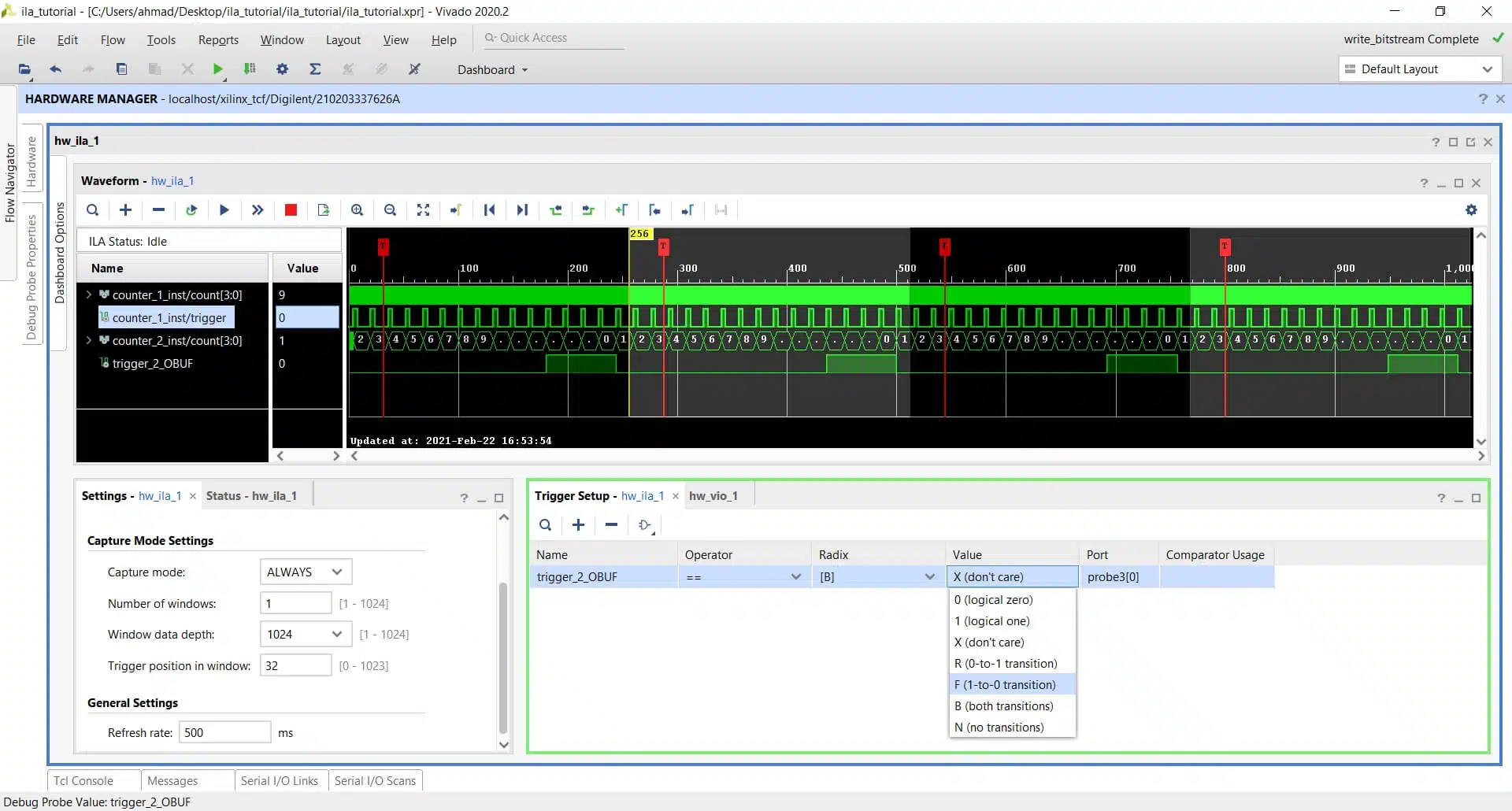
- Configure the trigger to the condition to equal (==) and falling edge F(1-to-0 transition)
- Configure the number of windows to 1 and FIFO depth to 1024, and position to 32:
- Click on Auto re-trigger button:
- Finally, change reset back to 0 from vio_reset:
We can see now that the waveform window is getting refreshed and updated as the trigger happen. It is fast, but the behavior is noticeable.
Click on Stop trigger and toggle Auto re-trigger.
Running ILA with Capture mode
Another feature of ILA is the Capture mode. In some cases, you are not interested in recording all the data but rather capture a specific sample. Capture mode helps you filter out data and record only the samples you are interested in.
Let’s say we are only interested in sampling when the output port trigger of counter_1_inst is ‘1’ AND the output port trigger of counter_2_inst is ‘0’.
To use Capture mode to achieve this, follow these steps:
- Change reset back to 1 from vio_reset
- Remove the previous trigger probe
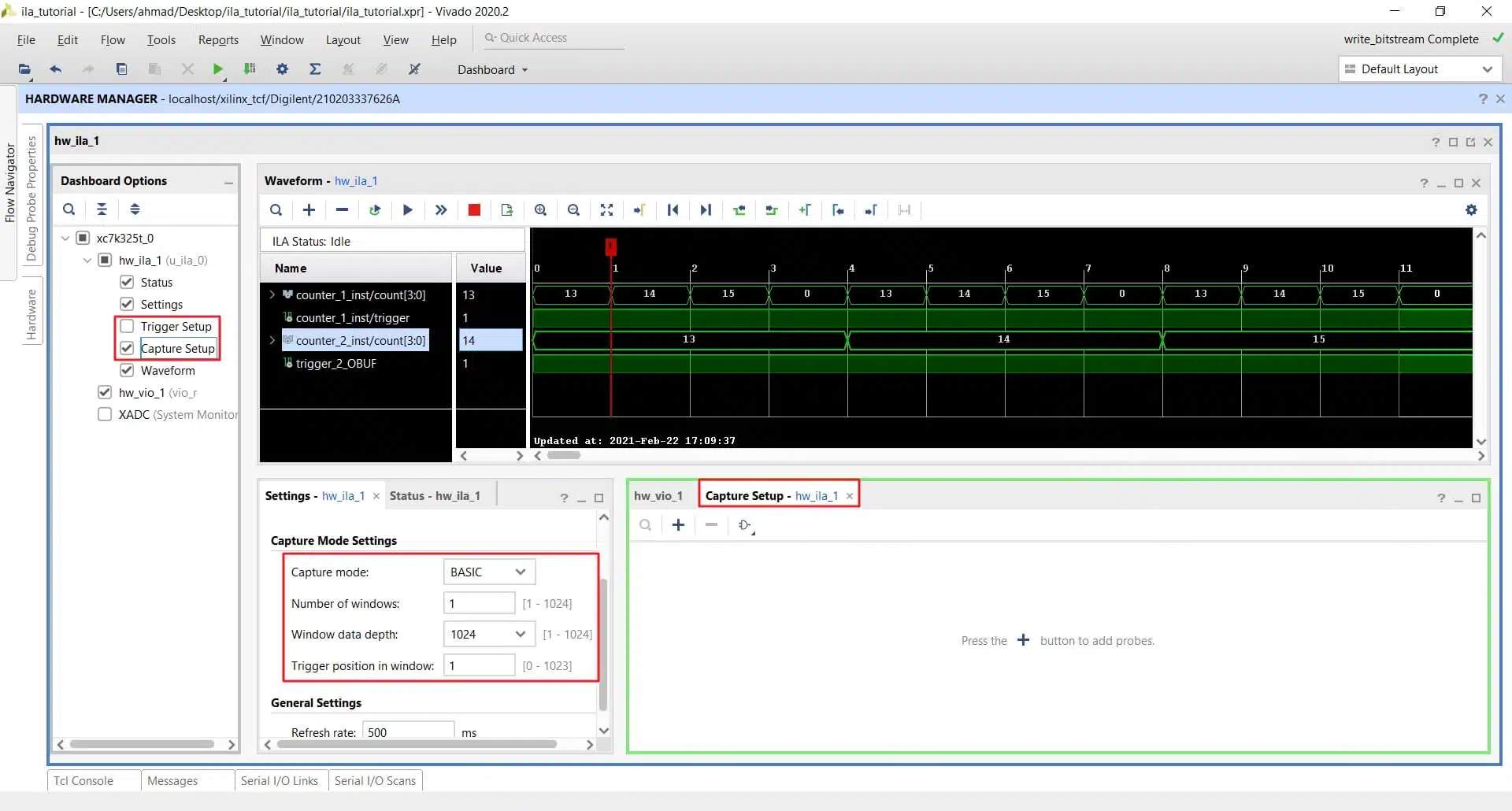
- From the dashboard, Uncheck Trigger Setup and check Capture Setup. Notice that a Capture Setup window will appear. From the Settings – hw_ila_1 window, Change Capture mode to BASIC, the window to 1, the FIFO depth to 1024, and position to 1:
- Add trigger_2_OBUF, and counter_1_inst/trigger from the Capture Setup window:
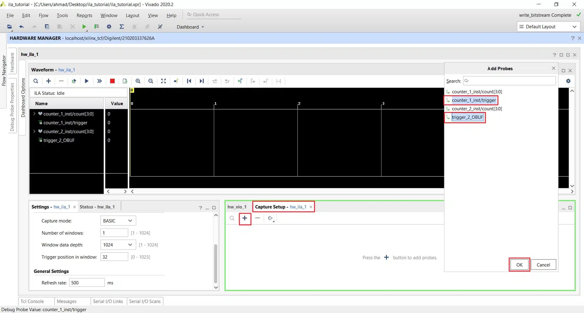
- Configure counter_1_inst/trigger to the condition equal (==) and 1 (logical one):

- Configure trigger_2_OBUF to the condition equal (==) and 0 (logical zero):
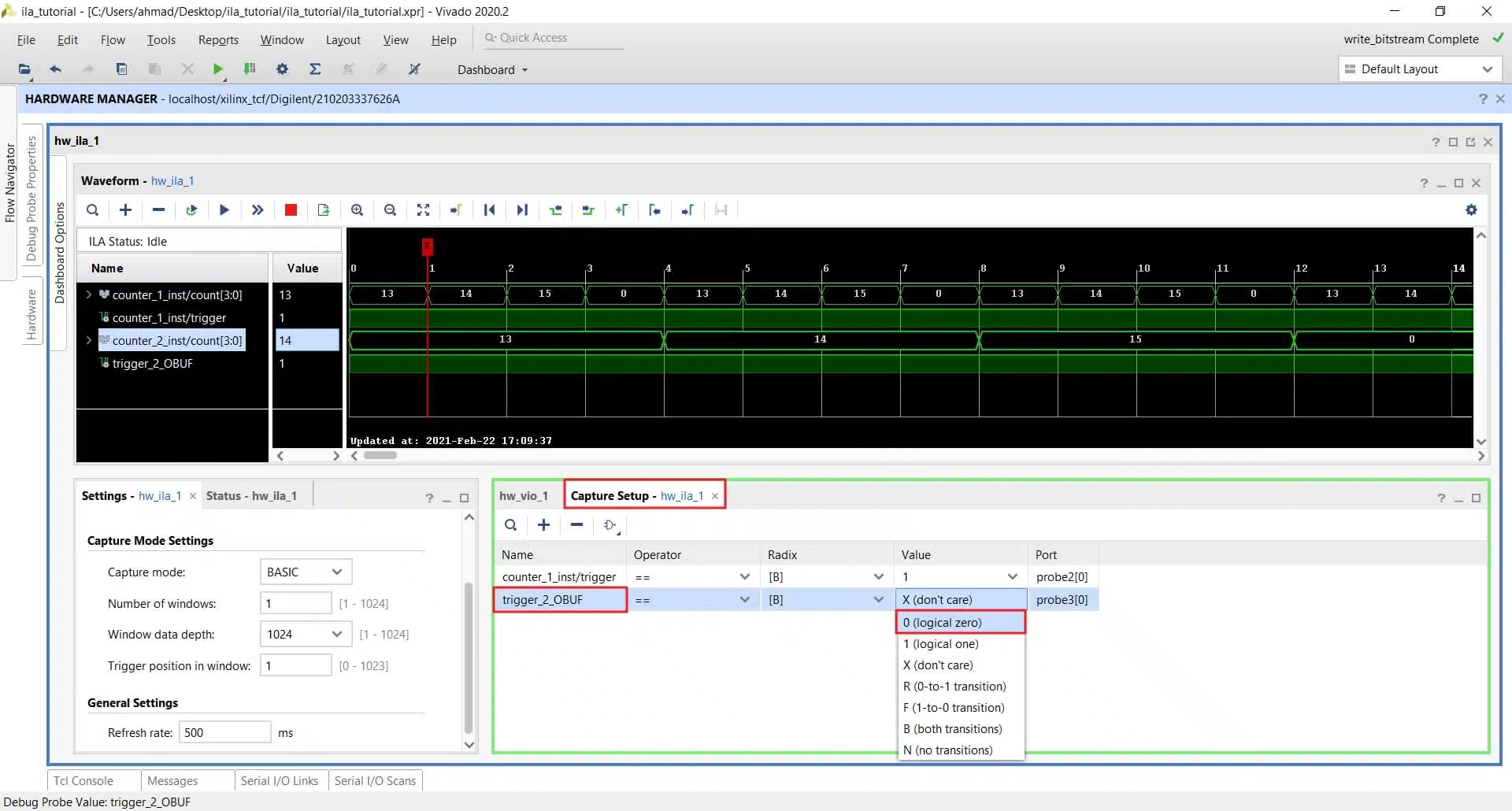
- Change the Capture Condition to Global AND:
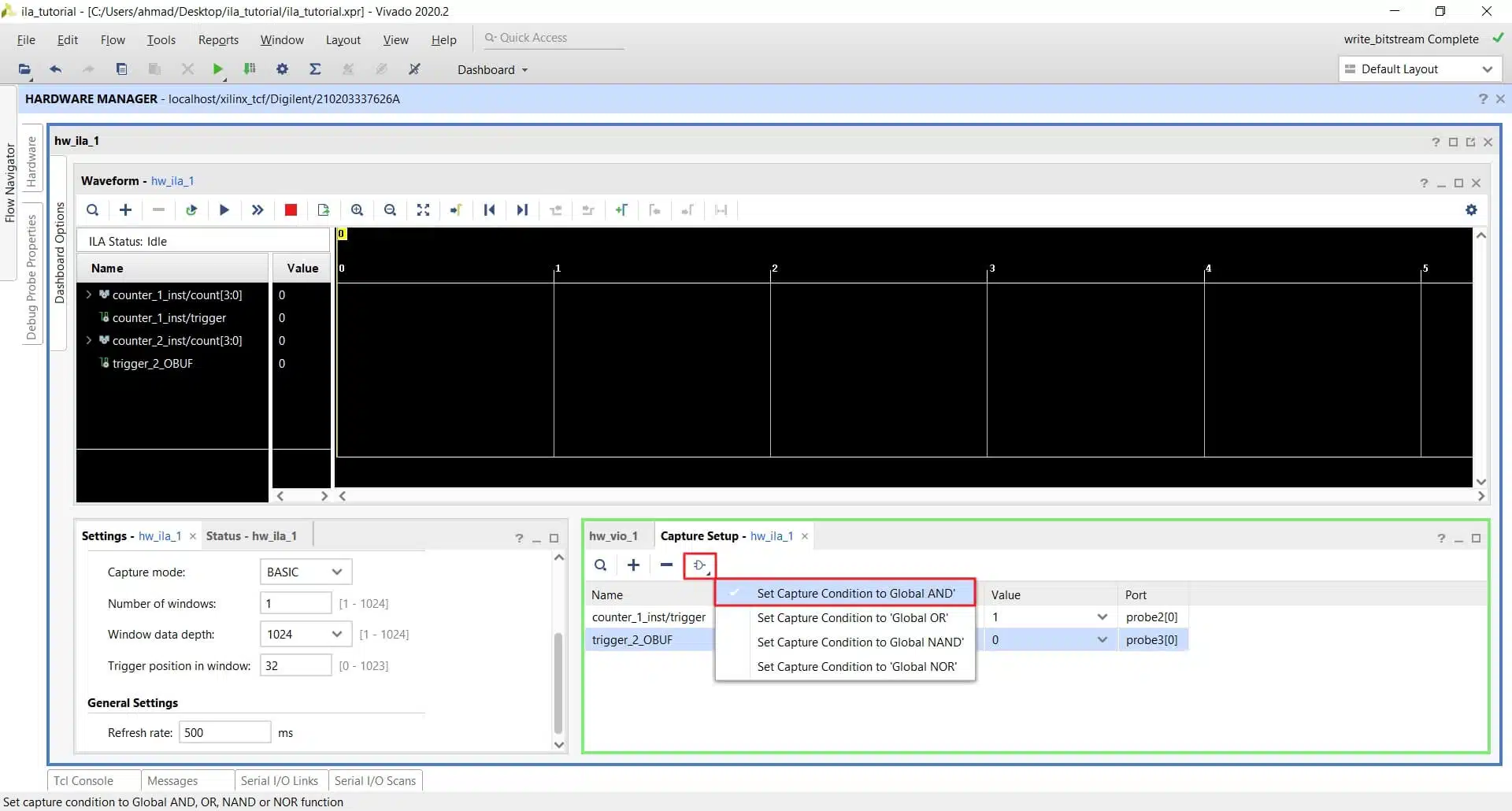
- Click on the Run trigger button and then change reset to 0 from vio_reset:
![Set reset ILA trigger value to "[B] 0"](https://cdn.vhdlwhiz.com/wp-content/uploads/2021/02/71.jpg.webp)
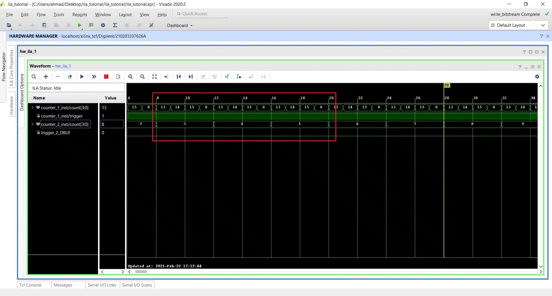
As we can see from the image below, the waveform has only recorded data when counter_1_inst’s count signal is 13, 14, 15, or 0. Any other counts are filtered out because counter_1_inst/trigger is high on these counts only.
Conclusion
In this tutorial, we learned about ILA and VIO and different use-cases for them. ILA and VIO are excellent options for on-chip debugging. They are free, easy to use, flexible, scalable, and simple yet offer advanced features. The use of multiple triggers and Capture mode helps you achieve a complex debugging scheme.

Dear Ahmad, thank you for a very interesting post. Speaking for myself I wasn’t even aware of these very helpful cores.
Do you happen to know if the cores are compatible with the Xilinx boards offered by Digilent? I’m thinking especially of this one
https://store.digilentinc.com/nexys-a7-fpga-trainer-board-recommended-for-ece-curriculum/
Apologies for asking directly rather than hunting all over the internet, but the Digilent boards are popular so I certainly hope so.
Yes it is compatible. It is just a normal IP that you can add to your design. Of course, you need to have space for it in your FPGA (enough BRAMs and LUTs). If you have a big design don’t choose a big fifo depth. If you have multiple clock domains, start with one clock domain so you don’t end up with two ILA core.
Hi, I am facing problems programming my FPGA board to incorporate both ILA and VIO in my HDL code. Can anyone help me with this? When I am connecting the ports of my design to both, I am facing an issue. Please help me resolve this. I have attached my code below:
`timescale 1ns / 1ps
//////////////////////////////////////////////////////////////////////////////////
// Company:
// Engineer:
//
// Create Date: 06/19/2021 05:22:39 PM
// Design Name:
// Module Name: addr
// Project Name:
// Target Devices:
// Tool Versions:
// Description:
//
// Dependencies:
//
// Revision:
// Revision 0.01 – File Created
// Additional Comments:
//
//////////////////////////////////////////////////////////////////////////////////
module addr(clk,a,b,cin,s,cout);
//parameter k=2;
input [1:0]a,b;
input cin;
input clk;
output reg [1:0]s;
output reg cout;
ila_0 ILA (
clk,
a,
b,
cin,
s,
cout
);
vio_0 VIO (
clk,
s,
cout,
a,
b,
cin
);
always@(posedge clk)
begin
{cout,s}=a+b+cin;
end
endmodule
The following error was shown:
[DRC 23-20] Rule violation (MDRV-1) Multiple Driver Nets – Net VIO/inst/PROBE_OUT_ALL_INST/G_PROBE_OUT[0].PROBE_OUT0_INST/probe_out0[0] has multiple drivers: a_IBUF[0]_inst/O, VIO/inst/PROBE_OUT_ALL_INST/G_PROBE_OUT[0].PROBE_OUT0_INST/Probe_out_reg[0]/Q.
I think you need to instantiate VIO and ILA from the generated instantiation template. When you generate VIO and ILA, vivado provide an instantiation template in the IP folder and you can copy and paste it in your design.
How do I add an active Free Running Clock so that ILA comes up after click Program?
I’m using the ZCU102 Eval Board.
Sorry for the late reply, you’ve probably figured it out already. One way is to create a block design with a Zynq7 Processing System (or ZYNQ UltraScale+ MPSoC) IP and use the FCLK_CLK0 clock.
Hi Jonas,
I had a Zynq Ultrascale+ MPSoC Block Design but wasn’t able to see the FCLK_CLK0 pin or even a place to enable it so I ended up using a fixed user clock connected to one of the banks in the 60’s. Then I set that user clock as the Domain Clock and then was able to get my ILA after clicking ‘Program’. I think the issue is that I didn’t initialize the Ultrascale+ which I was told to do it in the Vitis SDK but was wondering if I could initialize it in Vivado with a .tcl script instead.
A very instructive and detailed video. I wish a video like this was available at the Time I had my first I had to use ILA IP Core.
Cheers,
Rafael.