This article is by guest author Dimitar Marinov, whom I (Jonas) got in touch with after seeing his excellent videos about DSP filters. You can read more about Dimitry and find a link to his YouTube channel below the blog post. But first, read on to learn about FIR and IIR filters and the difference between the two.
This article is part of a series. Click here to read Dimitar’s other articles:
- Part 2: Finite impulse response (FIR) filters
- Part 3: FIR filter types
- Part 4: FIR filter testing
- Part 5: Polyphase FIR filters
Introduction
If you’re an HDL developer, chances are you’re going to encounter digital filters in some shape or form throughout your career. Hence this blog post serves as an introduction to the topic, seen from the eyes of a hardware developer.
This article discusses mainly the implementation of the filters rather than the theory and design. Therefore, it would be beneficial to have some basic understanding of the digital signal processing theory. If not, please refer to your favorite DSP book; mine is [1] 🙂.
FIR and IIR filter types
Digital filters are devices that modify the spectrum and phase of an input signal. Finite Impulse Response (FIR) and Infinite Impulse Response (IIR) are the two main types of digital filters you’re most likely to work with. Both are quite different from each other, yet they can be used interchangeably (in some situations).
The main difference between the two when it comes to implementation, however, is the signal path – FIRs are feed-forward-based (there are exceptions[1]), whereas IIR filters are based on a combination of feed-forward and feedback paths. This difference brings unique challenges when it comes to HDL implementation.
Filter building blocks
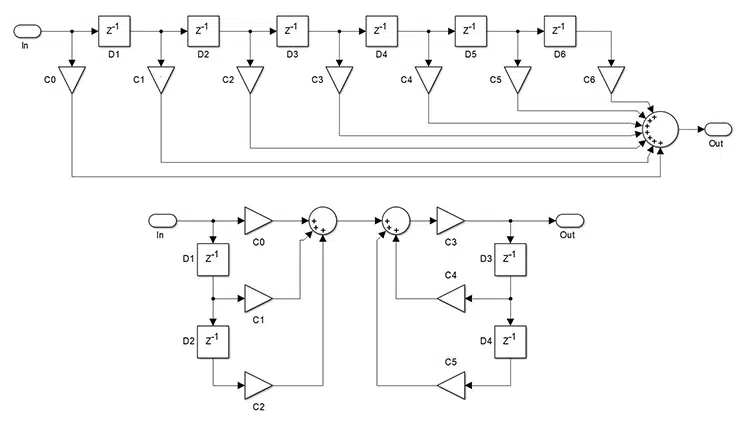
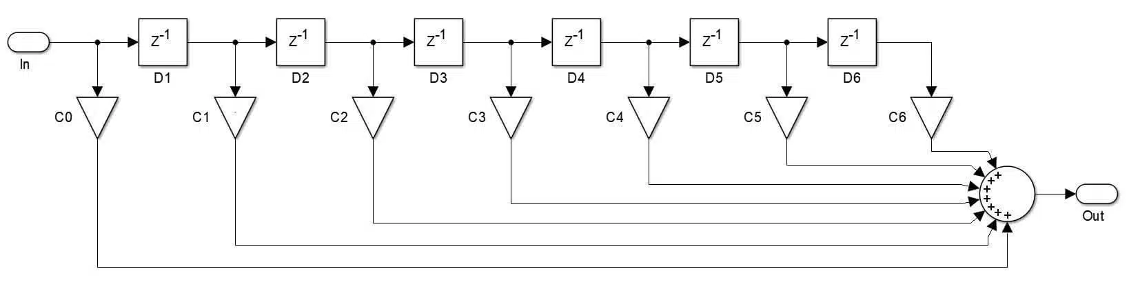
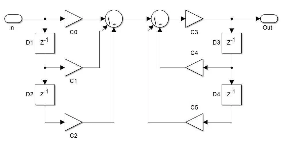
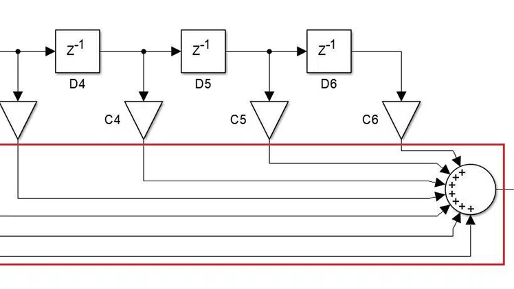
Figure 1 shows examples of FIR and IIR filter structures. The block diagrams specify the signal path and its operations, but not how they are implemented. Notice that both devices are composed of three main components – addition (the circles), multiplication (the triangles), and memory elements (the squares).
Memory elements
These are memory storage units that hold z-amount of consecutive data samples. For example, a delay element of z-1 holds one value, whereas z-N holds N-amount of values. When there are multiple delay elements in a row, the data is being shifted (transferred) from one element to the next once per sampling period. All memory elements connected sequentially form a delay line.
Arithmetic operators
The most common arithmetic operations involved in digital filters are addition and multiplication, with each using its own hardware. They are so common that some hardware allows them to perform a multiply-add operation, where both operations are performed at once. There are, of course, other operations such as division, logarithmic and trigonometric operations, but they are far less common.
Sampling rate
This is the rate at which the data is being processed by the filter, also known as sampling frequency or sampling clock/period (Fs). During this period, all operations (memory or arithmetic) are executed once.
Part 2: Finite Impulse Response Filters
Click here to view the follow-up article about FIR filters implemented using VHDL:
Part 2: Finite Impulse Response Filters
References
- [1] Richard G. Lyons, “11.5 Filtering Aspects of Time-Domain Averaging” in Understanding Digital Signal Processing


IIR works with feedback loops so picture 1b is wrong (copy of 1a).
I have updated the blog post with the correct image. Thank you for the heads-up!
I need to implement iir chebyshev 1 lowpass filter on fpga, order 6 , i need vhdl code for help , im using direct form 1 .