This terminology list explains words and phrases related to VHDL and FPGA development.
Use the sidebar to navigate if you are on a computer, or scroll down and click the pop-up navigation button in the top-right corner if you are using a mobile device.
Hit Ctrl+F (Windows/Linux) or Command+F (Mac) to search on this page.
Behavioral model
A behavioral model is a VHDL module that emulates another VHDL module or an external system in simulation. Behavioral models are often unsynthesizable.
The diagram below shows a testbench which contains two behavioral models.
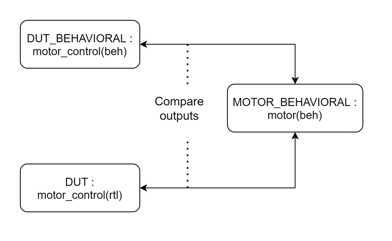
The model to the right emulates an external motor, providing feedback like angular data. And one above the device under test (DUT) acts as a blueprint to which we can compare the behavior of the RTL module.
If we implement it using unsynthesizable methods, for example, wait for statements or high-level VHDL features, it will be sufficiently different that we can use it to verify the DUT’s behavior.
Bitstream
A bitstream is a file that contains the configuration information for an FPGA. It is also known as a bit file or programming file because by streaming it to the FPGAs configuration port, we can program the FPGA.
The bitstream is a binary format, although sometimes it’s stored as a human-readable hex file. Common file suffixes for bitstreams are .bit, .bin, or .hex.
Bitstream generation happens after place and route, and it’s the last step of the FPGA design flow before physically programming the FPGA.
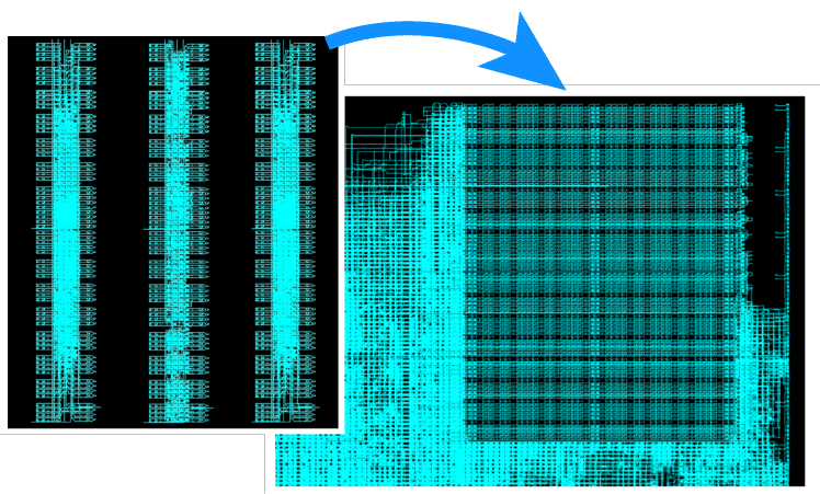
Block RAM
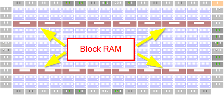
Block RAM (BRAM) is a type of on-chip random-access memory (RAM) found on most FPGAs. Usually, the chip provides rows or columns of BRAM distributed evenly throughout the floorplan, as shown in the example for the Lattice iCE40 device below.
The amount of block RAM varies greatly with the price of the FPGA. It can be as little as 32 kbits (Lattice LP640) or as much as 94.5 Mbits (Xilinx VU13P).
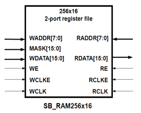
Dual-port block RAM is the standard for modern FPGA architectures. The term “dual-port” means that it supports simultaneous reads and writes of any two addresses. The image below shows the outline of a dual-port RAM from the Lattice iCE40 FPGA.
The CMOS technology in BRAM is different from the dynamic RAM (DRAM) used in regular computer memory. Block RAM is static RAM (SRAM), which doesn’t need refreshing. It doesn’t need a memory controller. Therefore, we can use each BRAM primitive individually to store data in our VHDL code.
True dual-port RAM means that both ports are interchangeable. While in simple dual-port RAM, one port is for reading and the other for writing, both ports can read and write in true dual-port RAM. Simultaneous writes to the same address usually result in undefined data.
Bus functional model (BFM)
A BFM is a behavioral model that replaces parts of your design or an external system. Its purpose is to mimic the missing subsystem so that you can successfully simulate the device under test (DUT).
For example, if your DUT is a network router, you can instantiate many BFMs to simulate other endpoints. When the DUT sends a package, the receiving BFM will send back an acknowledge (ACK) to satisfy the DUT, while in reality, the data doesn’t go anywhere.
Clock domain crossing
Clock domain crossing (CDC) means facilitating data transfer from logic governed by one clock net in the FPGA to logic in another clock net.
The two clocks may be skewed or have different frequencies, complicating timing closure. When one clock is faster than the other, steps must be taken to avoid data loss when transferring to the slower clock domain.
A common technique is to use a FIFO in block RAM to buffer data between the two sides. Dual-port block RAM is usually guaranteed safe to use with independent write and read clocks. You will have to handle the full/empty and address signaling using another scheme like Gray coding.
Clock net
A clock net or clock tree is a dedicated network of wiring and buffers optimized for routing a clock signal throughout the FPGA. From my master’s thesis, the image below shows a routed FPGA with one clock net highlighted in red.
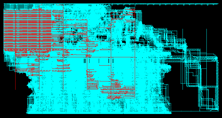
Clock buffers, also known as global buffers (BUFG), are primitives that can take a regular signal as an input and connect to a clock net on the output side. The buffers have a high fan-out to minimize skew while driving the numerous other primitives that utilize the clock signal.
Combinational logic
An RTL module or process that isn’t triggered by a clock edge is said to be combinational. The outputs are purely a function of the combination of inputs, thus the name combinational logic.
MUX_2_1 : process(sel, in_a, in_b)
begin
  case sel is
    when '0' =>
      out_q <= in_a;
    when '1' =>
      out_q <= in_b;
    when others =>
      out_q <= 'X';
  end case;
end process;
The process shown above describes a two-to-one multiplexer. It’s a combinational process because there is no clock input. The out_q signal reacts instantly when sel, in_a, or in_b changes.
The opposite of combinational logic is sequential logic.
Composite type
A composite type is a datatype consisting of several subelements. In VHDL, that can be either an array type or a record type.
Below are examples of composite types and composite signals. Note that the last signal is also a composite since std_logic_vector is an array of std_logic defined in the ieee.std_logic_1164 package.
  type arr_type is array (0 to 255) of real;

  type rec_type is record
    int_element : integer;
    slv_element : std_logic;
  end record;

  signal my_arr : arr_type;
  signal my_rec : rec_type;
  signal my_slv : std_logic_vector(31 downto 0);
Constraints
A constraint is a rule that dictates a placement or timing restriction for the implementation. Constraints are not VHDL, and the syntax of constraints files differ between FPGA vendors.
Physical constraints limit the placement of a signal or instance within the FPGA. The most common physical constraints are pin assignments. They tell the PAR tool to which physical FPGA pins the top-level entity signals shall be mapped.
Timing constraints set boundaries for the propagation time from one logic element to another. The most common timing constraint is the clock constraint. We need to specify the clock frequency so that the PAR tool knows how much time it has to work with between clock edges.
While there exist synthesis constraints, PAR constraints are far more common as they are mandatory while the former is optional.
Delta cycle
Delta cycles are zero-time timesteps used by VHDL simulators for modeling chained events during code execution. The outputs from a VHDL process with a sensitivity list will have outputs that lag behind the trigger signal with one delta cycle.
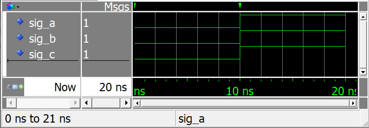
A delta cycle doesn’t consume simulation time. Consider the example code below with three concurrent VHDL processes. The sig_a signal changes from ‘0’ to ‘1’ after ten nanoseconds, causing the second process to wake up and copy the value to sig_b. Finally, the last process wakes up and copies the value to sig_c.
  signal sig_a, sig_b, sig_c : bit;

begin

  sig_a <= '1' after 10 ns;
  sig_b <= sig_a;
  sig_c <= sig_b;
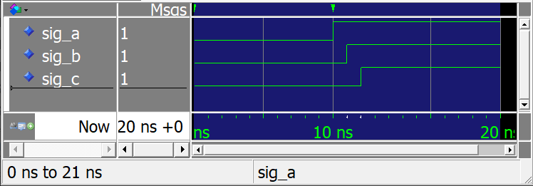
As we can see from the waveform below, the change is instantaneous. But behind the scenes, the VHDL simulator uses two delta cycle delays to model the chain of events.
If we turn on Expand Time Deltas Mode in ModelSim, we can observe the delta cycles, as shown below.
To learn more about delta cycles in VHDL, I recommend my in-depth article about it:
Delta cycles explained
Driver
A driver in VHDL is an instance or process that attempts to control the value of a signal. In the example below, the signal has three drivers: the process, the concurrent process, and the submodule.
process is
begin
  sig <= '0';
  wait;
end process;

sig <= '1';

MY_MOD : entity work.my_mod(rtl)
  port map (dout => sig);
It’s not possible to stop driving a signal once a process has started driving it. The exception is when you use the force command to override a signal’s value in the testbench. Then you can stop forcing it by using the release command, as shown below.
process is
begin
  sig <= force '0';
  wait for 10 ns;
  sig <= release;

  wait;
end process;
If the signal is of an unresolved type, driver conflict is a compilation error or a runtime error in the simulator. For resolved signals like std_logic or std_logic_vector, a resolution table determines the resulting value.
Read this article to learn the difference between resolved and unresolved types:
std_logic vs std_ulogic
Elaboration
Elaboration is the first part of the synthesis step in the FPGA implementation design flow. During elaboration, the synthesis tool scans the VHDL code and looks for descriptions of standard logic elements like flip-flops or multiplexers. The output from the elaboration step is a technology-independent netlist.
library ieee;
use ieee.std_logic_1164.all;

entity ent is
  port (
    sel, a, b : in std_logic;
    q : out std_logic
  );
end ent;

architecture rtl of ent is
begin

  q <= a when sel = '0' else b when sel = '1' else 'X';

end architecture;
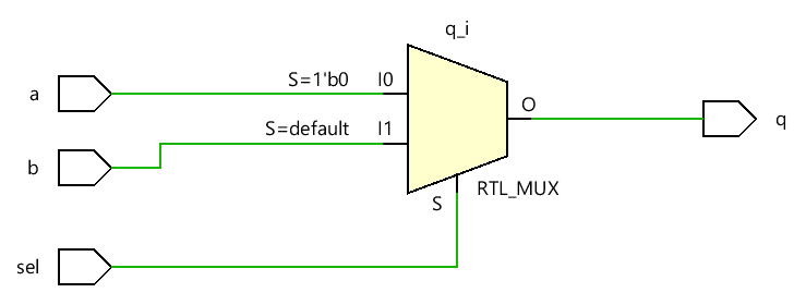
Consider the example VHDL code above. If we open it in Xilinx Vivado, we can issue the command synth_design -rtl to run only the elaboration step. As you can see from the RTL netlist below, Vivado correctly recognized the VHDL code as a multiplexer.
Fan-out
The fan-out for a primitive is the number of other logic elements connected to its output. When we say that a device like a buffer has high fan-out, it means that it’s capable of driving a large number of logic elements.
Hard core
With the term “hard core” in FPGA design, we mean a component implemented in a dedicated physical circuit. It’s most often used to describe a hard core CPU, but there are also hard cores for other elements like I2C controllers.
An example is the Xilinx Zynq-7000 FPGA, which contains one or two hard ARM Cortex-A9 processors and two hard master and slave I2C interface. The opposite of hard core is soft core.
Hard macro
A hard macro is a prerouted netlist designed for a specific FPGA architecture. It is possible to place the macro on different locations, but the footprint must precisely match the macro’s physical nets and primitives.
The image below is from my master’s thesis. It shows three hard macros with possible placements on a Virtex-6 FPGA.
Using hard macros can reduce the run time of PAR because the macro already gives the placement. Also, it may be desirable to control routing in timing-critical logic like Ethernet MACs. Therefore, it’s common to deliver such IP in a hard macro format.
Infer
The term “to infer” in FPGA design means intentionally describing a specific primitive with HDL code. The adept FPGA engineer knows how the synthesis tool “thinks” and can predict that it will map code written a certain way to the desired primitive.
The code below shows a process that will infer a flip-flop.
FDRE_PROC : process(c)
begin
  if rising_edge(c) then
    if r = '1' then
      q <= '0';
    elsif ce = '1' then
      q <= d;
    end if;
  end if;
end process;
The process precisely describes a D flip-flop with Clock Enable and synchronous reset, and therefore we can assume that the synthesis tool will choose this primitive on the FPGA. You can verify which primitive that was used by inspecting the synthesis log.
Inference stands in contrast to instantiation, where we specify the exact primitive through the entity or component instantiation methods in VHDL. The example below shows how to instantiate an equivalent D flip-flop in a Xilinx FPGA.
FDRE_INST : FDRE
port map (
  q => q,
  c => c,
  ce => ce,
  r => r,
  d => d
);
You are most likely to hear the term “inferred” to be used with either block RAM or latches. It can be tricky to infer block RAM, and therefore some engineers prefer to instantiate it instead. Inferred latches are almost always an undesirable effect of wrongly written code.
Latch
A latch is a logic element that can sample and hold a binary value. But unlike a flip-flop, which is edge-triggered, the latch is level-triggered. When talking about latches in the context of FPGAs, we usually mean the D latch, also called a transparent latch.
The animation below shows the logic gate equivalent of a transparent latch. It will let the Data (D) signal pass through when the Enable (E) input is ‘1’. When E is set to ‘0’, the value on the Q output is locked.
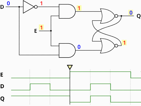
Latches are generally undesirable in FPGA design because they have inferior timing characteristics without offering any advantages over flip-flops.
Why latches are bad and how to avoid them
Click the link above to read more about latches!
Metastability
Metastability is an undesirable effect of setup and hold time violations in flip-flops where the output doesn’t settle quickly at a stable ‘0’ or ‘1’ value.
If the input changes too close to the triggering clock edge, the flip-flop output is undetermined. We can’t know for sure whether it’s going to be ‘1’ or ‘0’. Furthermore, the value may hover between the two binary states long enough the cause havoc in downstream logic. That’s metastability happening.
Consider the example below where a hold time violation on an external signal causes the input flip-flop to go metastable. Its output goes to the input of two other flip-flops. But because the output from the first flip-flop is metastable, it’s not a clear ‘1’ or ‘0’ when the downstream flip-flops sample the value. In the worst case, they might interpret the value differently.
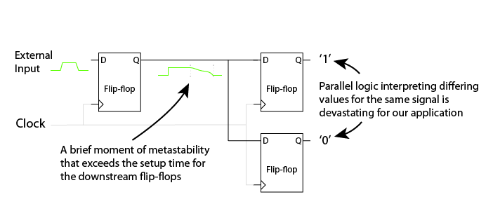
Metastability can result in an unpredictable circuit, and it’s hard to debug because the errors happen randomly. Fortunately, it’s easy to prevent.
We can reduce the probability of error to neglectable rates by cascading a few flip-flops at the input, as shown below. That gives the value time to settle before it reaches the critical logic.
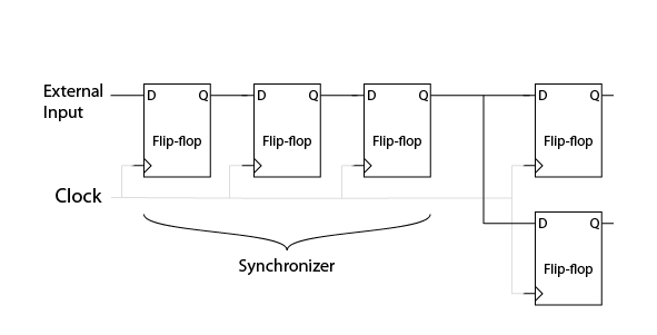
We call such a setup a synchronizer. The flip-flops are synchronizing the unsynchronized external signal to the internal clock.
The precise number of flip-flops needed depends on your design’s clock frequency and how long the physical signal path between the cascading flip-flops are. As a rule of thumb, three cascading flip-flops will prevent any possibility of metastability.
Multiplexer (MUX)
A multiplexer (MUX) is a basic digital logic element and a primitive found in FPGAs. The image below shows the two states of a two-input MUX. It acts as a switch, letting through either input signal, based on the selector input’s value.
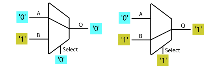
The binary 2-input type is the simplest possible MUX. But they can have several inputs, and the switched signals can be buses consisting of multiple wires.
The standard way to describe a MUX with VHDL is to use the Case-When statement.
Multiplier (DSP)
Multipliers are primitives in the FPGA capable of performing floating-point arithmetics. DSP block is an alternative name for a multiplier that reflects its primary use case in digital signal processing.
Not all FPGAs contain multipliers, but the number of DSP enabled slices ranges from less than ten to thousands for those that do.
Net
A net is a logical wire in a netlist. When designing VHDL, we often use multiple different signals when describing the same net. Consider the concurrent statement below, where we assign the value of one signal to another.
signal_a <= signal_b;
In the VHDL simulator, signal_a will follow signal_b after one delta cycle. But in reality, we are describing the same logical wire. The synthesis tool will merge such signal groups into a single net. Thus, it will have to create a new name for the combined net, usually a concatenation of the VHDL signal names.
Netlist
A netlist is a file format that describes the components, connectivity, and optionally, the placement and routing of an electronic circuit. In the context of FPGAs, there exist two main types of netlists: the unrouted netlist, and the routed netlist.
The unrouted netlist is the output from the synthesis step. We can also refer to it as a post-synthesis netlist. It contains an accurate description of the primitives in the design and how they are connected, but it lacks placement information.
The routed netlist, or post-route netlist, is the output from the place and route (PAR) step. It contains the same information as the unrouted netlist, but with added physical placements. It maps primitives and wires to exact locations on the target FPGA.
There also exist variations that have placement information but no routing. It’s also possible to have a partly routed netlist.
Primitive
Primitives are the smallest atomic logic element that we can configure on the FPGA.
Ultimately, most of the FPGA fabric consists of transistors, but we can’t address them individually with VHDL code or in any other way. We can only configure the components that they implement.
Examples of primitives are flip-flops, multiplexers, block RAM, and multipliers. Following this reasoning, other components like PLLs, Gigabit Ethernet transceivers, and even hard core processors, are also primitives. But it’s more common to refer to these complex units with their real names, rather than “primitives.”
Programming
It’s best to avoid the term “programming” when describing the activity of writing VHDL code because it’s misleading. We create digital logic with VHDL, not computer programs, so it’s better to say that you are “coding” or “designing.”
Furthermore, programming in this context refers to the last step in the FPGA implementation flow where we program the FPGA with the configuration data.
And finally, when we say “program the FPGA,” we mean to transfer the bitstream file to the FPGA board using a USB cable. We don’t mean writing VHDL code.
Register-transfer level (RTL)
When we say that a VHDL module is on the register-transfer level (RTL), we mean that it’s on the lowest abstraction level for FPGA development. Registers (flip-flops) are as far down the hardware stack as we can get on an FPGA.
We can’t configure transistors individually, but we can control the data flow through LUTs and registers. The RTL detail level includes how data moves between registers as time passes from one clock edge to the next.
In contrast to behavioral code, which is a higher abstraction level, RTL modules are most often synthesizable. Therefore, when FPGA engineers talk about “RTL code,” we usually mean modules that shall go on the FPGA.
Sequential logic
Sequential or clocked logic in VHDL is a process or component where the output changes on the clock signal’s active edge.
The output of a clocked process depends not only on the current state of the inputs but also on its previous values. Unlike a combinational process, a clocked process relies on the sequence of the inputs. Thus, the name sequential logic.
DELAY_PROC : process(clk)
begin
  if rising_edge(clk) then
    if rst = '1' then
      sig_p1 <= '0';

    else
      sig_p1 <= sig;

    end if;
  end if;
end process;
The code above shows a fully synchronous process that creates a copy of a signal delayed by one clock cycle. This code will infer a single flip-flop when synthesized.
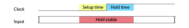
Setup and hold time
Setup and hold time describes how long the input signal must be stable before and after the triggering clock edge. The timing diagram below illustrates setup and hold time for a positive-edge triggered flip-flop.
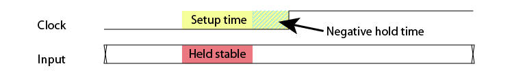
Furthermore, setup and hold times can be zero or even negative, but both properties cannot be negative simultaneously. The illustration below shows the effect of negative hold time; it shrinks the setup time requirement away from the clock edge.
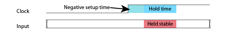
When the setup time is negative, the input is allowed to change after the clock edge, up to the hold time takes over, as shown in the image below.
Typically, we don’t have to specify setup and hold times for internal paths in the FPGA. The place and route tool has precise models of the FPGA architecture and can figure out the values automatically. But sometimes we have to override the default constraints, especially when dealing with clock domain crossing.
For external signals, we always have to think about setup and hold time. The router doesn’t know about the properties of external interfaces. We have to constrain them or manually or otherwise make sure that no timing violations happen.
Setup and hold time violations can lead to metastability.
Simulation
It’s difficult to debug VHDL code once it’s on the FPGA. The problem is that we have limited possibilities of gaining insight into the synthesized logic that’s not working.
The FPGA implementation flow is also a time-consuming process. The place and route tool can take hours or even days to route a large VHDL project. For these reasons, simulation of VHDL code is the only viable option for FPGA development.
A VHDL simulator is a software tool that interprets VHDL code and runs it like a computer program. VHDL is a hardware description language, but the simulator treats it like an event-driven parallel programming language.
Thus, the simulator doesn’t have to synthesize the code before simulating. It simulates the behavior of the VHDL code, not the hardware that it describes.
For this reason, the simulation can differ from the implementation. But the behavior of VHDL in simulation is clearly defined, and experienced VHDL designers will know how to avoid simulation mismatch.
I recommend reading the Delta cycle section and my in-depth article about delta cycles to understand better how the VHDL simulator works.
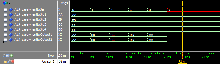
The simulation output is text printed to the console or a waveform view of selected VHDL signals in the design. The image above shows an example of a waveform from a multiplexer simulation.
Today’s most common VHDL simulators are Mentor Graphics’ ModelSim/QuestaSim and the build-in simulator in Xilinx Vivado. There are few open-source options, but one is the GHDL project.
We don’t usually simulate VHDL modules stand-alone, but rather through a dedicated VHDL simulation program called a testbench.
Single-event upset
A single-event upset is when the natural background radiation causes an erroneous value in a digital logic element. It’s caused by an ionizing particle hitting a nano-scale logic element in the FPGA.
The phenomenon is very improbable. Still, engineers have to make sure that it doesn’t cause a disaster when designing safety-critical electronics for aerospace or space applications.
Countermeasures against single-event upsets include one-hot encoding of state machines with a fallback “safety” state. Or the complete FPGA could be made radiation-hardened with triple modular redundancy.
Soft Core
The term “soft core” refers to a component implemented using the configurable resources of the FPGA. It’s most commonly used to describe a soft core microprocessor, but other elements can also be soft cores.
Examples of soft core processors are Xilinx Microblaze or Intel Nios II. An example of a non-CPU soft core is an I2C Bus Master Controller generated by Vivado IP Catalog.
Synthesis
Synthesis is the FPGA implementation design flow step that maps VHDL code to a technology-dependent netlist. The software responsible for performing synthesis is called a synthesis tool.
The synthesis tool analyzes the VHDL code and figures out a way to implement the described logic using the primitives available on the target FPGA. The first substep of synthesis is elaboration.
If successful, the output is a netlist that describes the primitives, and the interconnect between them. But this netlist lacks information about the placement of components and routing. That is the subject of the next implementation step: place and route.
library ieee;
use ieee.std_logic_1164.all;

entity ent is
  port (
    sel, a, b : in std_logic;
    q : out std_logic
  );
end ent;

architecture rtl of ent is
begin

  q <= a when sel = '0' else b when sel = '1' else 'X';

end architecture;
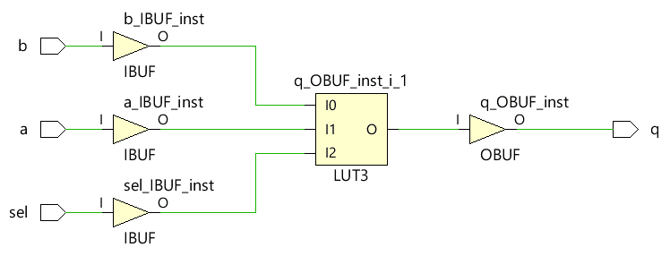
The example code above describes a multiplexer. If we synthesize it in Xilinx Vivado, we will get the synthesized netlist shown in the schematic below. The netlist implements the multiplexer as a top-level module using primitives specific to the Spartan-7 FPGA.
Testbench
A testbench is a VHDL module whose purpose is to let us simulate another module.
All RTL modules depend on external stimuli to function. That may be input signals from another module or the clock signal from outside of the FPGA. They also have output signals. Without them, it would be no point in creating the module in the first place.
Having the device under test (DUT) as the top module in simulation is problematic. The issue is that the signals are leaving the VHDL domain, so we would have to interact with them using a different coding language, for example, Tcl.
To avoid this problem, we instead create a separate testbench VHDL module just for the simulator. Because the testbench is supposed to be the top module in the simulation project, its entity is usually empty. It’s a self-contained unit with no signals entering or exiting.
Instead, it contains local signals and an instance of the DUT. Additionally, it has code that generates the DUT’s input stimuli, for example, the clock signal. This system is the deliberate intention of VHDL’s creators; the language contains large portions meant only for simulation.
We refer to any such VHDL module as a testbench, even though it doesn’t always test anything. If the verification relies on human interaction, we call it a manual-check testbench.
A self-checking testbench, on the other, is an automated test program. It’s like a unit test for VHDL; it runs through a test suite and prints out “OK” or “Not OK” in the end.
The example code below shows a self-checking VHDL testbench for an inverter module.
library ieee;
use ieee.std_logic_1164.all;
use std.env.finish;

entity inverter_tb is
end inverter_tb;

architecture sim of inverter_tb is
  signal a, q : std_logic;
begin

  DUT : entity work.inverter(rtl)
  port map (
    a => a,
    q => q
  );

  SEQUENCER_PROC : process
  begin

    a <= '0';
    wait for 10 ns;
    assert q = '1' report "q = 0" severity failure;

    a <= '1';
    wait for 10 ns;
    assert q = '0' report "q = 1" severity failure;

    report "Testbench finished: OK";
    finish;
  end process;

end architecture;
Read this article to learn more about self-checking testbenches:
How to create a self-checking testbench
Translate
The term “translate” is ambiguous, even within the FPGA context.
In the Xilinx design flow, “translate” refers to the process of merging synthesis netlists and constraints before PAR. Or it could mean to migrate a native netlist to a generic type, and vice versa.
-- synthesis translate_off

sig <= 'H';

-- synthesis translate_on
Another use of the term is in the VHDL code, as shown in the listing above. The synthesis tool will ignore the code between the translate_off and translate_on tags. Thus, you can add code to your RTL modules that don’t appear in the implemented design.
Verification
Verification means to generate proof that your application matches the specification.
For example, we can verify a VHDL module by using a testbench in a simulator environment. Or we can run a post-implementation simulation to check that the design is sane after PAR. And finally, we can verify that the programmed FPGA works by testing it in the lab.
Hungry for more? Join the Fast-Track!👇
Are you familiar with programming but new to VHDL?
Do you need a short introduction to this unfamiliar subject?
Is your schedule full with no time left to study?
Understand the basics of FPGA development using VHDL in a few evenings! This course is for IT professionals and students who need a fast run-down of the subject. With this course and the low-cost Lattice iCEstick development board, you will be developing real hardware within hours.
Click here to read more and enroll:
FPGA and VHDL Fast-Track: Hands-On for Absolute Beginners